
Architecture
This page describes how the ADK is put together and why. It covers the geometric axis, which is what this release ships; What the ADK is sets out both axes of assembly verification. Most of the structure below follows from one decision: the assembly rules must not know any fabrication layer number of any PDK. Everything else, the adapters, the boundary manifest, the shared registries, exists to make that decision hold.
The role model
The ADK sits one abstraction layer above all PDKs.
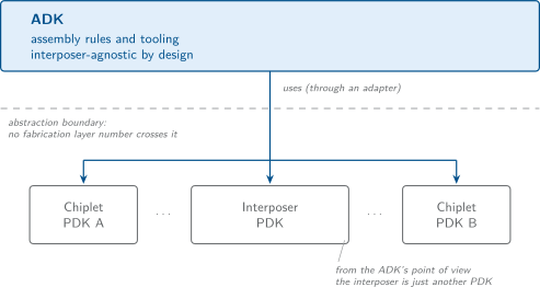
The role model. The ADK sits one abstraction layer above every PDK and reaches each one only through an adapter.
Each PDK owns its own fabrication rules, and the ADK governs only the
interactions between chiplets and the interposer. The consequence worth stating
explicitly is that the interposer is just another PDK from the ADK’s point of
view. The IHP IntM4TM2 fabrication rules
(Padc_*, TM*, TV*) live inside the interposer repository, and the
ADK never touches them. The ADK reaches the interposer only through an adapter,
the same way it would reach any other substrate.
Note
Several version numbers are in play and they are deliberately independent.
The adapter contract, the config/*.json registries, the package
VERSION file and the ADK README.md all read 0.2.0, the
release in which the interconnect axis landed. The boundary-manifest schema
version (1.0.0) is a separate axis, pinned on its own. The ADK’s
CHANGELOG.md is the authoritative record of what has landed, and a test
in the ADK enforces that VERSION and every config/*.json version key
match its latest released entry.
The abstraction boundary
Rules under klayout/drc/rule_decks/ and templates under
kicad/dru/templates/ reference abstract input names only. The mapping
from an abstract name to a PDK-specific fabrication layer lives in the adapters
under pdk_adapters/, and nowhere else.
Three abstract inputs exist today.
Name |
Status |
Source |
Semantics |
|---|---|---|---|
|
required, adapter-declared |
interposer adapter |
The region the interposer offers for chiplet attachment.
|
|
injected |
boundary manifest |
The mechanical outline of each placed chiplet, built from the
manifest’s |
|
optional |
interconnect adapter |
The region the attachment method’s pitch and spacing rules check.
Defaults to |
chiplet_attachment_input is semantic, not technology-specific. On the
IHP IntM4TM2 interposer it is derived from Cu pillars, formed where the
passivation opening and the final Cu pad overlap:
passiv_pillar = polygons(9, 35)
dfpad_pillar  = polygons(41, 35)

chiplet_attachment_input = passiv_pillar.and(dfpad_pillar)
That is the entire executable content of
pdk_adapters/interposer/intm4tm2.drc; the rest of the file is its SPDX
header and a comment saying which mechanism the region models. On a
different substrate the same abstract input might be built from solder-bump
openings, or from a hybrid-bonding pad array. The rule never cares which, which
is what lets one rule deck check assemblies built on substrates the deck has
never heard of.
Why there is no chiplet adapter
The tempting symmetry, “if there is an interposer adapter then there should be a
chiplet adapter”, is deliberately rejected, and the asymmetry is about what is
present in the assembled GDS. The
interposer’s fabrication geometry is in the assembled layout, because the
assembly is drawn on the interposer’s metal stack, so rules need a way to talk
about that geometry abstractly. Chiplet internals are different. Where they are
present in the assembled GDS at all, and hyp_to_gds.py does read each die’s
layout in and instantiate it, they are drawn in that die PDK’s own layer
numbers, which the ADK deck has no portable way to interpret. For assembly
checking a placed chiplet is therefore represented only by
chiplet_boundary, a mechanical outline carried by the boundary manifest.
There is no chiplet-side layer stack for an adapter to map.
The 4 assembly rules the deck ships treat all chiplets uniformly through that boundary and need nothing more:
ASM.a, chiplet boundaries must not overlap.ASM.b, minimum chiplet-to-chiplet spacing.ASM.e, minimum chiplet area, a degenerate-polygon sanity check.ASM.f, attachment geometry that overlaps a chiplet boundary must sit fully inside it.
None of them can be improved by knowing which PDK a chiplet came from.
If a future use case does appear, for example “a chiplet of type X must expose its declared bump pattern”, the mechanism will be designed against that actual need rather than scaffolded in advance.
config/chiplet_pads.json reinforces the same reasoning: it records the pad
vocabulary the black-box generator emits, sits on the producer side rather than
on the assembly check, and no ADK rule reads it. See Registries and schemas.
Adding an interposer
A new interposer plugs in by adding one adapter file under
pdk_adapters/interposer/. Nothing in the rule decks is edited.
Selection happens at run time:
at the DRC runner,
--interposer-adapter <name>, resolved againstpdk_adapters/interposer/or taken as an explicit path to a.drcfile;through the orchestrator, from the
.chipletassembly file’sinterposer.adapterfield.
The same resolution applies in the KiCad DRU generator, so the two toolchains select the same adapter by the same name. Adapter contract gives the full contract and a worked example of writing one.
The interconnect axis
The interconnect axis is a second, orthogonal adapter axis. Where the interposer axis answers where attachment lands, the interconnect axis answers how dense, by what method: the bump-to-bump pitch and spacing that are a property of the bumping method (Cu pillar, solder bump, microbump) rather than of the substrate.
An adapter under pdk_adapters/interconnect/ is a parameter pack. It sets
entries in the interconnect_rules dictionary and declares no fabrication
layer at all. The 8_2_interconnect.drc deck then applies the IXN rules
over ixn_region, which is interconnect_region when an adapter narrowed it
and chiplet_attachment_input otherwise.
Composing the two axes is what gives full modularity. Swap the interposer adapter to change the substrate. Swap the interconnect adapter to change the bumping vendor. Neither touches the other, and the ADK rules are unchanged either way.
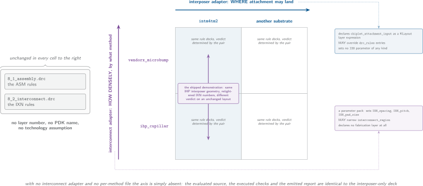
Two orthogonal adapter axes. The interposer axis says where attachment may land, the interconnect axis says how densely, and neither touches the other or the rule decks.
The axis is optional and additive, and that is a structural guarantee. With no interconnect adapter and no per-method file, the eval chain is
layers_def.drc -> interposer adapter -> validation -> 8_1_assembly.drc
which is byte-identical to the deck as it stood before the axis existed:
8_2_interconnect.drc is simply not concatenated. The interconnect axis
governs the attachment method, not chiplet contents, so it leaves the “why
there is no chiplet adapter” reasoning intact. Interconnect rules (IXN) gives the
conditions under which each part is appended.
The eval chain
klayout/drc/adk_assembly.drc is a wrapper, not a rule deck. It resolves
paths, loads the registries, parses the boundary manifest, and then assembles
the deck as a single Ruby string that it evaluates once. Reading the source
in that order explains most of the contract:
Load
config/layers.jsonandconfig/rule_params.jsoninto the localsadk_layersanddrc_rules. Both files must exist or the run aborts.config/interconnect.jsonis loaded intointerconnect_rulesif present, and tolerated if absent so that a partial checkout still runs the interposer-only path.Resolve the chiplet boundary source. Unless
legacy_exchange0is set, a boundary manifest is mandatory: the wrapper raises if-rd manifest=is missing or the file does not exist, and parses it intoboundary_manifest.Require an interposer adapter. A missing or non-existent
-rd adapter=aborts the run.Optionally accept an interconnect adapter, and optionally a per-method interconnect file. When the per-method file is present, every method entry is checked for
IXN_spacing,IXN_pitch,IXN_pad_sizeanddies, and the boundary manifest becomes mandatory because legacy mode carries no per-die instance names.Concatenate the parts and
evalthe result.
The concatenation is literally a list of file contents and generated source joined with newlines:
layers_def.drc              chiplet_boundary, from the manifest or, in
                            compat mode, from the legacy exchange0 layer
<interposer adapter>        declares chiplet_attachment_input;
                            MAY override drc_rules entries
<generated validation>      raises unless every required input is
                            defined? and non-nil
<interconnect adapter>      only if one was selected; sets interconnect_rules
<generated validation>      only if one was selected; raises unless every
                            required IXN_* key is present
8_1_assembly.drc            the ASM rules
8_2_interconnect.drc        only if an interconnect adapter and/or a
                            per-method file was loaded; the IXN rules
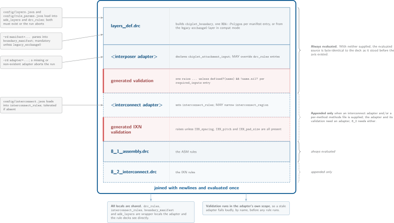
The eval chain. The deck is assembled as one Ruby string and evaluated once, which is why every local is shared and why the interconnect axis is purely additive.
Two properties follow from doing this as one eval rather than as separate
loads, and both are load-bearing:
All locals are shared.
drc_rules,interconnect_rules,boundary_manifestandadk_layersare wrapper locals that the adapter and the rule decks see directly. That is why an adapter can overridedrc_rules['ASM_b']with a plain assignment, and why the rule decks can usedefined?(...)to detect optional inputs.Validation runs in the same scope as the adapter. The required-input check is generated Ruby source, one
raise ... unless defined?(name) && !name.nil?per entry ofrequired_inputs, spliced in immediately after the adapter. A stale adapter therefore fails loudly, by name, before any rule runs.
The required list is a single line in the wrapper:
required_inputs = ['chiplet_attachment_input']
The interconnect validation is built the same way from
['IXN_spacing', 'IXN_pitch', 'IXN_pad_size'], and checks presence in the
interconnect_rules dictionary rather than definedness of a local.
Cross-tool consistency
The KLayout deck and the KiCad DRU generator are separate implementations that must agree on what they check. They agree because they read the same registries and apply adapter overrides the same way.
config/rule_params.json and config/interconnect.json are shared. The
KLayout deck loads them into drc_rules and interconnect_rules; the KiCad
generator loads the same defaults and merges the adapter’s literal numeric
overrides, but only when invoked with the matching adapter flag, so without the
flag you get the registry defaults rather than the adapter’s view.
KiCad DRU generation gives the merge grammar and its consequences.
The agreement covers the one ASM parameter both tools consume, ASM_b.
ASM.a is left to KiCad’s native courtyard collision check, ASM.e and
ASM.f have no KiCad equivalent, and the template emits no IXN constraint
at all, because the interconnect checks are post-layout geometry checks; the
interconnect adapter’s name appears in the generated file only as a provenance
comment. See KiCad DRU generation.
config/layers.json is legacy-compat only. The wrapper always loads it but
consults its exchange0 entry only on the --legacy-exchange0 path; the
KiCad generator does not read it at all.
The chiplet boundary itself travels in a per-assembly manifest described by
config/schema/boundary_manifest.schema.json. Producers emit it next to the
assembly GDS, the DRC runner discovers or accepts it and injects it with
-rd manifest=..., and klayout/macros/boundaries_to_rdb.py renders the
same manifest as a .lyrdb so the Marker Browser shows exactly the polygons
the rules saw. Because the manifest lives outside any fabrication-layer
namespace, the assembly contract is PDK-agnostic by construction and no
(190, 0) literal survives in the default path.
Boundary manifest is the normative description.
Known limitations
These are properties of the current design, not defects to be worked around.
The ASM rules assume a single tier.
chiplet_boundary is a flat 2D region. The boundary manifest records placement
polygons with no z coordinate, and layers_def.drc merges every polygon into
one region with no per-die identity. ASM.a therefore flags any XY overlap
between chiplet boundaries, including the case of dies legally stacked at
different z in a multi-tier assembly. The assumption is baked into the manifest
data model, not only into the rule: lifting it would need a z-aware manifest
schema (a version bump), per-die identity in layers_def.drc, and a
tier-aware ASM.a. The KiCad-side mirror, native courtyard collision, is
equally 2D. This is not a practical constraint today, because nothing in the
toolchain produces multi-tier assemblies.
Note
The per-method interconnect path does reconstruct per-die identity, because
it rebuilds one region per method from the manifest instance names. That
identity exists only inside 8_2_interconnect.drc; the ASM rules still
see a single merged region.
Die z consistency is checked at export, not in the deck.
The KLayout deck sees only 2D geometry plus the manifest, so it cannot check
heights at all. The rule “each die’s position.z equals the mounting surface
plus its connection-stack height” is enforced by the 3Dblox exporter,
openroad/chiplet2dbx.py, which compares the two to a tolerance of 1e-6 um
and refuses to export an assembly that does not satisfy it exactly. Downstream,
read_3dbx in OpenROAD loads the exported model and check_3dblox lints
its geometry; the exporter deliberately grounds the substrate so that the
floating-chip check has a reference. An assembly that is never exported gets no
automated z check. See OpenROAD 3Dblox export and
Verification stages.