
Overview
This page is the map of the whole flow. Read it once before starting, then work through From die GDS to KiCad onwards.
What goes in and what comes out
The flow takes three kinds of input:
- Die layouts.
One GDSII per chiplet you intend to place. Only the external pad layer and the text layer that names those pads are actually consumed, so a stripped or black-boxed die works as well as a full one. The dies keep their own PDKs, and the flow never checks their internals.
- An interposer technology.
A KLayout technology describing the substrate the dies are mounted on: layer properties (
.lyp), a technology file (.lyt), a layer map and the technology’s own fabrication rule decks. IHP-GmbH/OpenIntM4TM2 is the reference implementation, the IHP 130 nm IntM4TM2 aluminium BEOL interposer.- An interconnect technology.
A manifest of chiplet attachment methods (Cu pillar, solder bump, vendor microbump), each with its stack geometry and its pitch and spacing numbers. IHP-GmbH/IHP-Interconnect-IntM4TM2 is the reference implementation. It is a separate, swappable axis from the interposer: the interposer fabricates the pad openings, the interconnect method fills them.
It produces:
<board>.chiplet, the assembly description that names every component, its technology, its position in three dimensions and its attachment method.<board>_interposer.gds, the fabrication-oriented interposer layout, and<board>_complete.gds, the same layout with every die instance placed into it.Machine-readable sidecars: a boundary manifest and a pillar manifest next to each GDS the converter writes, plus an interconnect-method sidecar next to the complete GDS.
DRC reports: a KLayout
.lyrdbfrom the ADK assembly deck and a JSON summary from the Cu-pillar check.
Warning
The kit is a Preview Release. The assembly checks described here are the geometric axis of assembly verification: placement, spacing, minimum area, attachment geometry and bump pitch. They do not reconcile the assembled layout against a system netlist. That connectivity axis is within the kit’s scope but is not part of this preview release. They also do not replace the per-PDK fabrication DRC that each die and the interposer still need in their own technologies.
The flow at a glance
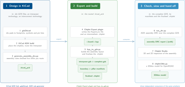
The design flow, from die layouts and an interposer technology through to a checked assembly. The eight stages are grouped into three phases, and the numbers match the stage table below.
The same pipeline, seen as the files each stage consumes and writes:
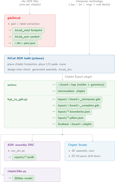
The flow in artefact terms. Each stage names the tool that runs it and the files it writes.
The stages
# |
Tool |
Input |
Output |
Documented in |
|---|---|---|---|---|
1 |
|
Die GDS plus a layer-properties file |
|
|
2 |
KiCad ADK build ( |
Footprints, symbols, interposer technology |
|
|
3 |
|
ADK rule parameters plus the selected adapters |
|
|
4 |
Chiplet Export plugin |
The loaded |
|
|
5 |
|
|
Interposer GDS, complete GDS, manifests, finalised |
|
6 |
|
Complete GDS plus its boundary manifest |
|
|
7 |
Chiplet Studio |
|
Interactive 3D and 2D inspection |
|
8 |
|
|
A 3Dblox model for OpenROAD |
Stages 4 and 5 are one action in practice. The export dialog writes the
HyperLynx file and the intermediate .chiplet, then invokes
hyp_to_gds.py as a worker subprocess, and stage 6 runs immediately
afterwards over the complete GDS when that output is enabled. They are listed
separately because they consume and produce different artefacts, and because
hyp_to_gds.py also runs standalone.
The pivot artefact: .chiplet
The .chiplet file is the one artefact every tool reads, and it is what makes
the pipeline a pipeline rather than a chain of one-off converters. It is YAML,
human-readable and diffable, and carries four groups of information:
assemblyandinterposerThe design name, the working units, and the interposer adapter the assembly DRC should use.
technologiesEach technology the assembly touches, with the path to its layer properties file and its database unit. Paths may be written with
${VAR}references, for example${INTERPOSER_PDK_ROOT}/libs.tech/klayout/tech/intm4tm2.lyp, which readers expand through the shared discovery chain.connection_stacksandinterconnectThe attachment methods in play, each expanded to its physical layer stack (material, height and diameter per layer). The values are copied from the interconnect PDK manifest, so a
.chipletstays readable even where that PDK is not installed.componentsOne entry per interposer and per die: technology, layout path, top cell, outer dimensions including thickness, position in x, y and z, rotation, and for a die its
connectionmethod and itsorientation. The interposer entry also carries the extractedio_pads.
A die’s position.z is not a free parameter. It is the attachment surface
plus the height of the selected connection stack, and the 3Dblox exporter
refuses assemblies where the two disagree.
The file passes through two states: the KiCad writers emit an intermediate
version carrying a _metadata.finalize_required: true marker, and
hyp_to_gds.py rewrites it in place once the interposer GDS exists, anchoring
positions to the canonical frame and stripping the marker. Readers refuse a file
that still carries it, so a half-finished export cannot be mistaken for a
finished one.
The .chiplet assembly file and Components and optional blocks are the field-by-field reference, and Coordinate frames explains the frame the finalised file uses.
What the assembly checks actually check
The rule decks are technology-agnostic: the interposer adapter says where on the substrate attachment may land, and the interconnect adapter says how densely bumps of a given method may be placed there.
That gives 4 assembly rules and 7 interconnect
rules over the assembled GDS, plus a design-time subset mirrored into KiCad as
a .kicad_dru. Architecture explains the split,
Assembly placement rules (ASM) and Interconnect rules (IXN) list the rules, and
Verification stages explains which check runs when and what
each one cannot see.
Project layout
The flow expects a design to be laid out with a clean split between authored source and generated products:
my_design/
  kicad/       KiCad source you author: .kicad_pro, .kicad_sch, .kicad_pcb,
               the project .pretty library, .kicad_sym, fp-lib-table
  chiplets/    die GDS inputs and their pin lists
  outputs/     export products: <board>.chiplet + MANIFEST.md at the root,
               GDS layouts and sidecars under layout/,
               DRC reports under reports/
adk-new-project <name> scaffolds exactly this, together with a
.gitignore that tracks the light deliverables and ignores the heavy
regenerable ones. The reference design ships in the same shape, so anything
that works there works in a scaffolded project without rewiring.
Where to go next
Tip
If you want to see the whole flow work before running any of it yourself, open the reference design described in Reference design. It is a two-die assembly on the IntM4TM2 interposer, regenerated and DRC-gated on every build of the tools image, so its outputs are known good.
No toolchain yet: The ADK-Tools image.
Toolchain installed, starting from your own dies: From die GDS to KiCad.
Unfamiliar with the vocabulary: Glossary.
Adding a new interposer or a new bumping vendor: Adapter contract.