
Viewing and inspecting
Three viewers cover the assembly at three levels. Chiplet Studio shows the assembly as a stack of physical bodies and lets you drill into any component’s real layout. KLayout shows the assembly GDS itself, with named and coloured layers when the interposer technology is registered. The KLayout Marker Browser walks a result database, either the violations from an assembly DRC run or the chiplet boundaries rendered from the boundary manifest.
Opening the assembly in Chiplet Studio
The entry point is the .chiplet file, not a GDS:
chiplet-studio outputs/two_die_interposer.chiplet
Launched with no argument the application opens an empty session and you load the file from File > Open.
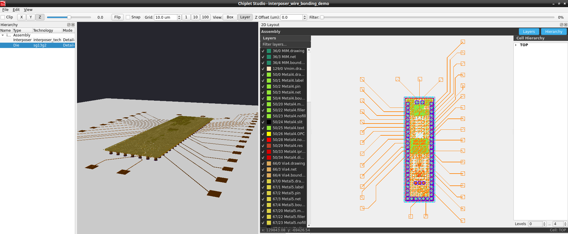
Chiplet Studio: the 3D assembly view on the left, the 2D view in assembly mode on the right with its layer panel and cell hierarchy. The capture is of a simplified single-die demo, not of the two-die reference design.
How the file resolves its layouts
A .chiplet references layouts by path, and those paths are resolved against
the .chiplet file’s own directory. In the reference design the interposer is
layout/two_die_interposer_interposer.gds and each die is
../chiplets/Metal_Test.gds, so the whole project moves as one directory
tree with no absolute paths to fix up. Studio also picks up the assembly GDS
from that same layout/ directory when it is present. Paths written as
${INTERPOSER_PDK_ROOT}/... or ${GDS_TO_KICAD_ROOT}/... are expanded on
read through the discovery chain; see Environment and path discovery.
What the panels give you
The Hierarchy dock on the left lists the assembly’s components with their type and technology, plus the interconnect method rows: an assembly-level row for the bumping method and, under each die, the method that die actually uses. Selection is synchronised with the 3D view in both directions.
The Properties tab, docked beside 2D Layout, shows the selected component’s geometry with unit conversion. Selecting an interconnect row shows the method’s stack instead.
The render mode is per component. Right-click a hierarchy row and pick from
Render Mode: Wireframe, Transparent, Detailed (with Si bulk) and
Detailed (no Si bulk). The last two tessellate the component’s real GDS,
which is how you see routing and pads as bodies rather than as a box. The
interposer starts in an opaque Solid mode and dies start Transparent.
Hiding a component is the checkbox on its hierarchy row, not a render mode.
Chiplet Studio lists what each mode draws.
The toolbar carries two controls worth knowing. Filter hides polygons below an area threshold for the selected component, which makes a detailed die readable by dropping fill and small shapes. Layer Z spreads a stackup apart vertically for inspection; it is a visualisation aid only, does not change the saved model, and is enabled only for a single imported die, because fanning out a multi-component assembly would interleave the stacks.
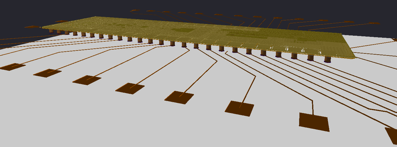
A lateral view: the die sits on its Cu pillars above the interposer body, with the wire-bond I/O pads and the traces fanning out to them at the interposer edge.
Drilling down into a component’s layout
Double-click a component, in the hierarchy or in the 3D view, to open its
layout in the 2D Layout dock. Studio loads the component’s layout file
with the layer properties declared by the component’s technology, and
navigates to its top_cell. This is a real KLayout view: the layer panel on
the left is the technology’s layer table with the usual visibility toggles, the
cell hierarchy is on the right, and the status bar tracks the cursor in microns.
The Back button is context dependent. From an individual die’s layout it returns to the assembly layout; from the assembly layout it resets to the full top-level view, undoing any hierarchy navigation you did in place. Closing the dock returns you to the 3D view alone.
Tip
If a die opens without colours, its technology is missing a
layer_properties entry, or the .lyp that entry points at did not
resolve. The reference design declares two technologies, intm4tm2 for
the interposer and sg13g2 for the dies, each with its own .lyp.
Other panels
View > Net Graph inspects the assembly connectivity. View > Flow Pipeline
runs the build steps declared in the .chiplet’s flow: block against the
assembly, which is how the 3Dblox export and its linter can be driven from the
GUI. View > Python Console, or Ctrl and the backtick key, opens an
embedded interpreter with a chiplet_studio module for scripting the
assembly. File > Export PNG renders the current 3D view.
Opening the GDS in KLayout with named layers
An assembly GDS opened in a plain KLayout session is a stack of numbered layers. Registering the interposer technology gives every layer its name and colour from the PDK layer table:
klayout -n intm4tm2 outputs/layout/two_die_interposer_complete.gds
In the ADK-Tools image this works out of the box: KLAYOUT_PATH already
includes the interposer tree, so intm4tm2 appears in KLayout’s technology
selector and -n intm4tm2 resolves. The registration is nothing more than
putting the directory that holds libs.tech/klayout/tech/intm4tm2.lyt and
intm4tm2.lyp on the search path.
Outside the image, do the same by hand:
export KLAYOUT_PATH=$HOME/.klayout:/path/to/OpenIntM4TM2/libs.tech/klayout
klayout -n intm4tm2 two_die_interposer_complete.gds
Note
Keep a writable directory as the first entry of KLAYOUT_PATH. KLayout
treats it as its configuration home and will not start cleanly if the first
entry is read only. The image uses /tmp/.klayout for exactly this
reason.
Tip
Do not put the base SG13G2 PDK on KLAYOUT_PATH; its PCell autorun macro
pops error dialogs in a GUI session. The interposer tree ships its own autorun
pymacro, which bootstraps the intm4tm2 PCell library and is why the
ADK-Tools image puts that tree on the path deliberately. hyp_to_gds
reaches the SG13G2 PCells through PDK_ROOT, a different mechanism. See
Installing on the host.
Walking DRC violations in the Marker Browser
An assembly DRC run writes a KLayout result database. With --run_dir it
lands there as <layout-stem>_<topcell>_assembly.lyrdb; the export pipeline
names it after the board, as in
outputs/reports/two_die_interposer_assembly_drc.lyrdb.
To inspect it:
Open the GDS the run checked, with the interposer technology.
Tools > Marker Browser.
Load the
.lyrdbfrom the browser.
The browser lists one category per rule, using the rule identifier and its
message as they were rendered at run time, for example ASM.b : Min.
chiplet-to-chiplet spacing is 50.0 um or IXN.x.cupillar_opt1.vendorx_microbump
: Min. cross-method spacing ... is 40.0 um. Selecting an item zooms the layout
to the offending geometry.
A category with no items is a rule that ran and found nothing, so the category list is a record of what was checked; read it before concluding that a rule you expected was actually evaluated. The reference design’s committed report carries eleven rule categories and no items.
Viewing chiplet boundaries
Chiplet boundaries are not in the GDS; they travel in the
<gds-stem>.boundaries.json manifest, so opening the assembly GDS shows the
dies’ artwork but not the mechanical outlines the assembly rules actually check.
The boundaries_to_rdb macro closes that gap: it reads the same sidecar the
DRC runner injects and renders it as markers, so what you see is exactly what the
checker sees. Nothing is written into the GDS.
From the command line:
python klayout/macros/boundaries_to_rdb.py \
    outputs/layout/two_die_interposer_complete.gds
Pass the assembly GDS and the sidecar is auto-discovered next to it by the same
rule the runner uses; pass the manifest .json directly if it lives
elsewhere. The output is a .lyrdb next to the manifest, or wherever -o
says. Load it in the Marker Browser exactly like a DRC report.
From the GUI, make the macro discoverable and use the menu entry:
export ADK_ROOT=/path/to/IHP-Open-ADK
export KLAYOUT_PATH=$HOME/.klayout:$ADK_ROOT/klayout:/path/to/OpenIntM4TM2/libs.tech/klayout
Then open an assembly GDS and run Tools > Show chiplet boundaries (ADK boundary
manifest). One click builds the same database in memory and loads it into the
Marker Browser. Symlinking
klayout/macros/show_boundaries.lym into ~/.klayout/macros/ works too.
The database has one chiplet_boundary category with a sub-category per
placed chiplet, named by its instance and described by its source die. Markers
are drawn from polygon_dbu, the field the DRC treats as authoritative,
converted to microns using the manifest’s own database unit, so they land on the
layout regardless of the layout’s own resolution.
Note
The viewer pins the manifest version it understands and refuses a sidecar
that does not match, rather than rendering an older schema approximately.
If it complains, regenerate the sidecar with a current hyp_to_gds.
There is also a producer-side option, hyp_to_gds --annotate-boundaries,
which paints the boundaries onto a viewer-only GDS layer. Prefer the marker
database: it needs no regeneration, adds no synthetic geometry to a layout you
may hand off, and cannot be mistaken for something a rule reads. See
Generating the assembly GDS.