
Coordinate frames
A .chiplet file carries XY positions that originate in several different
coordinate frames: KiCad’s PCB frame, the HyperLynx file’s absolute frame, and
the GDS frame. A die placed in the wrong one lands tens or hundreds of
micrometres off its pads, and the resulting layout still looks plausible. Six
alignment incidents in the reference toolchain traced back to exactly that.
The coordinate-frame contract is the response. It pins one canonical frame,
requires every writer to convert into it, and requires every reader to fail
loudly when something leaks through un-converted. It is normative: it is part
of the .chiplet format definition, it lives in the IHP-GmbH/chiplet-spec repository
at docs/coord_frame_contract.md, and where it and the format specification
could appear to differ, the contract governs.
Any tool may implement the contract under any license. It is a format-level companion to the schema, not the property of one implementation.
Warning
This is the single most common source of subtle placement bugs in the flow, and the failures are silent. Nothing downstream of a wrongly framed position can detect that it is wrong: the GDS is well formed, the DRC deck checks what it is given, and the 3D view renders happily. The only defence is that every writer converts and every reader range-checks.
The rules in brief
All
positionx and y values in a.chipletfile are expressed in the GDS-bbox-corner frame of the interposer top cell, y-up cartesian, micrometres.positionis the component’s geometric centre in x and y, not its corner. In z it is the seating plane, the bottom face of the placed body.Each component declares an explicit
anchor:gds_originfor a mesh built around the component’s own GDS(0, 0),bbox_centerfor a mesh centred on its own GDS bounding box.Z-mounting is per-die. Each die’s
connectionselects its own bump or pillar bodies, so one assembly can mix methods.hyp_to_gds.py --update-chiplet-fileis mandatory in the canonical path. KiCad’spcbnewGUI export produces an intermediate file whose positions are in the wrong frame.Interposer
dimensionsare the board outline (prBoundary 235/0, drawn from KiCad Edge.Cuts) when that layer is present;positionstays the full-GDS-bbox centre.
The canonical frame
Property |
Value |
|---|---|
Reference object |
The interposer’s GDS top cell |
Origin |
Lower-left corner of the interposer’s GDS bounding box |
X axis |
Increases rightward |
Y axis |
Increases upward (y-up cartesian) |
Units |
Micrometres |
Float precision |
At least six decimal places, that is 1 pm in theory |
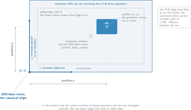
The canonical frame. Positions are measured from the lower-left corner of the interposer’s GDS bounding box, in micrometres, y up.
Why the GDS bbox corner
The choice is not arbitrary, and the alternative was tried.
The GDS file is the physical fabrication artefact. The interposer GDS is the ground truth of the layout.
KLayout, the 3D scene in Chiplet Studio, and any downstream packaging tool all consume positions as offsets within the GDS bbox.
The PCB Edge.Cuts bounding box, which KiCad uses natively, does not always match the GDS bbox. The wire-bond demo historically carried a hidden shift of (-200 um, -780 um) between the two, even though the widths and heights agreed to the micrometre. The GDS frame is the only one with no such hidden shift relative to what actually gets fabricated.
Because the converter draws the board outline (Edge.Cuts into prBoundary 235/0) into the interposer GDS, the GDS bbox contains the outline. In the normal case, where all drawn geometry sits inside the outline, the canonical origin coincides with the outline’s lower-left corner and the historical shift is zero by construction.
Position semantics
position x and y are the component’s geometric centre. For a die of width
1000 um and height 2000 um whose lower-left corner sits at (250, 250) inside
the interposer:
position:
  x: 750.0      # 250 + 1000/2
  y: 1250.0     # 250 + 2000/2
  z: 57.83      # seating plane, see the z-mounting rule below
dimensions:
  width: 1000.0
  height: 2000.0
  thickness: 50.0   # body spans z 57.83 to 107.83
position.z is the seating plane: the bottom face of the placed body, the
face that meets the mounting surface. For a die on a connection stack, that is
the tip of the stack. dimensions.thickness extends the body upward from
position.z.
Note
Files that predate real thickness data carry the placeholder
thickness: 0.0, where the centre reading and the seating-plane reading
of position.z coincide. With a real thickness they differ by
thickness / 2, and the seating-plane reading is the normative one: it
is what the z-mounting rule computes and what consumers implement.
Interposer dimensions against interposer position
The interposer is the one component whose dimensions and position come
from different sources and answer different questions.
Field |
Source |
Meaning |
|---|---|---|
|
bbox of prBoundary 235/0, the board outline drawn from Edge.Cuts, when that layer is present; bbox of all drawn geometry otherwise (legacy GDS) |
The fab extent of the interposer, which is what viewers render as the substrate body |
|
KiCad stackup ( |
The interposer’s physical body z-extent, silicon substrate plus BEOL.
It extends downward from |
|
Interposer stackup |
The die-attachment surface in the interposer-local frame, the plane
dies mount on. Optional; consumers fall back to
|
|
Half of the full GDS bbox, all layers including the outline |
Where the mesh bbox centre sits in the canonical frame, consistent with
|
When the outline contains all drawn geometry, the full bbox equals the outline
bbox and both fields describe the same rectangle. When copper leaks outside the
outline, which is a design error and which the converter warns about loudly at
export, dimensions keeps the true board size while position follows the
mesh centre. That preserves die and pillar registration in the render at the
cost of a shifted substrate body.
The anchor convention
Each component declares how its local mesh is built. The anchor is declared by the writer, based on knowledge of how that component’s GDS was produced. The reader must not infer it from the component type.
Value |
Meaning |
Use cases |
|---|---|---|
|
The mesh is built around the component’s own GDS |
Dies produced by |
|
The mesh is centred on the component’s own GDS bounding box.
|
Interposers. Components whose GDS layout uses absolute pcbnew-derived coordinates and whose meaningful placement reference is the geometric centre. |
If anchor is absent, the reader must default to bbox_center and warn.
That path exists for legacy files only; there is no auto-migration, and new
files must declare the field. The reference implementation collects the
defaulted components and emits one file-level summary rather than one warning
per component, so a legacy file produces a single readable line naming every
component that was defaulted.
Note that gds_to_kicad’s footprint convention is the reason dies declare
gds_origin. The tool sets the footprint reference text at (at 0 0),
placing the footprint origin at GDS cell (0, 0), and places pads at their
GDS-derived centres relative to that origin. The die’s GDS (0, 0) is
therefore the reference point KiCad uses, and the .chiplet anchor has to
say so.
Orientation and flip-chip mirroring
A flip-chip die is mounted face down: its active layers and BEOL point at the interposer, and the connection stack carries every pad across the gap.
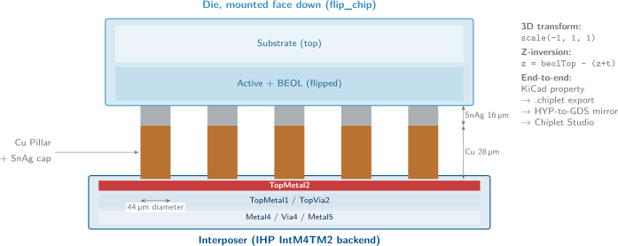
A flip-chip die in cross-section, seated on Cu pillars with SnAg
caps over the interposer’s TopMetal2. The die’s active face points down at
the interposer, and that physical fact is what the flip_chip mirror
described below encodes in plan view.
orientation takes exactly two canonical values.
Value |
Meaning |
|---|---|
|
The die artwork is used as drawn, with no mirror. Applied before
|
|
The die is mounted face-down onto the interposer, realised as an
x-mirror of the die artwork ( |
``face_down`` is not a canonical token. Flip-chip mounting is expressed as
flip_chip, because the mirror is the observable contract while “face down” is
only the physical picture. Writers must emit face_up or flip_chip and
nothing else.
Readers split on what to do with a non-canonical token:
Validators and exporters must reject it. An ambiguous token must never silently yield wrong geometry. In the ADK,
pads_vs_pillarsandchiplet2dbxboth raise a hard error onface_downand on any unknown string.Interactive viewers may be lenient and keep rendering, but must warn, and may treat
face_downasflip_chip. A viewer must never silently render an unknown token asface_up, because un-mirrored is the one answer that looks fine and is wrong.
The flip is realised as a mirror in x only, never in y. A pad that sat on the
left of the die layout therefore ends up on the right of the assembly, which is
the whole reason the mirror has to be applied before any pad is compared
against a pillar. gds_to_kicad --flip-chip implements it as
mx = -1 if flip_chip else 1, generating the footprint as seen from the
interposer side.
From a die-local coordinate to an assembly coordinate
This is the arithmetic every consumer has to get right. A pad or bump lives in
the die’s own GDS frame, in micrometres, y-up, with the origin at the die’s GDS
(0, 0), which is what anchor: gds_origin declares. To compare it
against anything in the assembly, for example the pillar positions in the
pillar manifest, it has to be mapped into the canonical frame:
global = position + R(rotation.z) * M * local
with
M = diag(-1, 1)   for orientation: flip_chip
M = diag( 1, 1)   for orientation: face_up

R(a) = [ cos a   -sin a ]
       [ sin a    cos a ]
The order matters: mirror first, then rotate, then translate by the die’s
position. Applying the rotation before the mirror gives a different answer
for every angle that is not a multiple of 180 degrees.
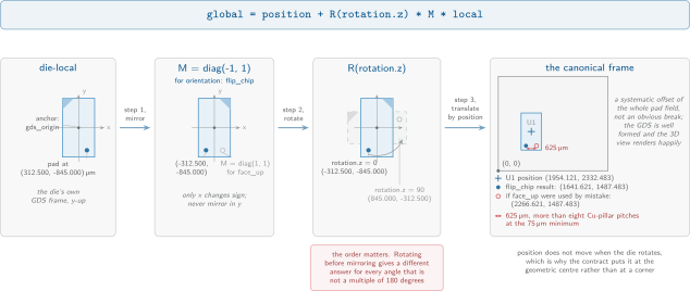
Mirror first, then rotate, then translate. Applying the flip-chip mirror in the wrong place moves the whole pad field by a fixed offset and leaves the layout looking plausible.
Worked case
Take die U1 from the reference assembly:
- id: U1
  type: die
  anchor: gds_origin
  orientation: flip_chip
  connection: cupillar_opt1
  position: {x: 1954.121, y: 2332.483, z: 57.83}
  rotation: {z: 0.0}
and a pad whose centre in the die’s own GDS is (312.500, -845.000) um.
Step 1, mirror. orientation: flip_chip means M = diag(-1, 1), so
the local coordinate becomes (-312.500, -845.000). Only x changes sign.
Step 2, rotate. rotation.z is 0, so cos a = 1 and sin a = 0 and
the vector is unchanged.
Step 3, translate.
x = 1954.121 + (-312.500)*1 - (-845.000)*0 = 1641.621
y = 2332.483 + (-312.500)*0 + (-845.000)*1 = 1487.483
The pad sits at (1641.621, 1487.483) um in the canonical frame.
Had the same die been face_up, step 1 would have left x at +312.500 and
the pad would land at (2266.621, 1487.483): 625 um away, which is more than
eight Cu-pillar pitches at cupillar_opt1’s 75 um minimum. This is the error
mode that makes a flip-chip mistake look like a systematic pad-to-pillar offset
rather than an obvious break.
Now rotate the same flip-chip die by 90 degrees, rotation: {z: 90.0}. Then
cos a = 0, sin a = 1, and the mirrored local vector
(-312.500, -845.000) transforms as:
x = 1954.121 + (-312.500)*0 - (-845.000)*1 = 1954.121 + 845.000 = 2799.121
y = 2332.483 + (-312.500)*1 + (-845.000)*0 = 2332.483 - 312.500 = 2019.983
giving (2799.121, 2019.983) um. Note that position did not move: the
die’s geometric centre is rotation invariant, which is precisely why the
contract puts position at the centre rather than at a corner.
Tip
pads_vs_pillars implements this transform in transform_pads() and
is the cheapest way to find out whether your understanding of a die’s
placement agrees with the toolchain’s. It compares every transformed pad
against the pillar manifest and reports the ones that do not match within
tolerance. See Pad to pillar alignment.
The 3D world frame
A viewer maps the canonical frame into its own world frame. Chiplet Studio’s OpenGL world is y-up in millimetres, with z out of the screen, so the mapping is an axis permutation plus a sign flip and a unit change:
geometry.transform.translate(
    static_cast<float>(pos.x / 1000.0),    // chiplet X -> 3D X (mm)
    static_cast<float>(pos.z / 1000.0),    // chiplet Z -> 3D Y (mm)
    static_cast<float>(-pos.y / 1000.0));  // chiplet Y -> 3D -Z (mm)
The synthetic contract fixture checks this with no tolerance at all: an
interposer at (500, 500, 0) um must map to (0.5, 0.0, -0.5) mm, and a
die at (250, 250, 50) um to (0.25, 0.05, -0.25) mm.
The z-mounting rule
For dies that mount on a connection stack, whether Cu pillar, solder bump or microbump:
z_die = mounting_surface + connection.total_height()
where mounting_surface is the z_bottom of the interposer stackup layer
whose name matches the connection stack’s first layer, after the
interconnect-PDK fragment for this die’s connection has been merged in, and
connection.total_height() is the sum of height over every layer in the
stack.
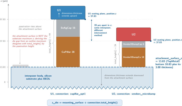
The z-mounting rule. A die’s seating plane is the attachment surface plus the total height of its own connection stack, so two dies with different methods sit at different heights on the same interposer.
How the mounting surface resolves
Taking cupillar_opt1 on the IntM4TM2 interposer:
Take the die’s connection id,
cupillar_opt1.Load the interposer stackup,
intm4tm2, and merge the interconnect fragment for that connection id. The fragment declaresz_reference: attachment_surface, so itsCuPillarlayer, at local z 0.00, is offset by the stackup’sattachment_surface_zof 13.83. After the merge,CuPillar.z_bottom = 13.83.The first layer name of the stack is
CuPillar. Look it up in the merged stackup. It is found, somounting_surface = 13.83.z_die = 13.83 + total_height(cupillar_opt1).
The merge happens per die and before the first-layer lookup, which is what makes the rule per-die: a die using any method seats on that method’s body heights even when its neighbours use other methods.
Worked case, two dies and two methods
Die |
|
Stack layers |
|
|
|---|---|---|---|---|
U1 |
|
CuPillar 28 + SnAgCap 16 |
44 |
57.83 |
U2 |
|
VendorXBumpCu 18 + VendorXBumpCap 6 |
24 |
37.83 |
Both dies sit on the same interposer, whose attachment surface is at 13.83, and
they end up 20 um apart in z because their interconnect differs. U1 selects
Option 1 rather than Option 2 because its pad ring contains a 79.93 um-pitch
pair, which is legal at Option 1’s 75 um minimum but below Option 2’s 80 um.
That selection lives in the die’s footprint CONNECTION field in KiCad and
rides through the export unchanged.
Edge cases
Case |
Behaviour |
|---|---|
Die has no |
Mount on |
|
Same as above. |
The connection’s first layer is not in the interposer stackup, even after the fragment merge |
Mount on |
|
Use |
Die has |
Use the explicit value. Do not auto-calculate. |
Every fallback lands the die on the BEOL top. None of them returns 0: an
earlier implementation did, and it put every die at world z = 0, which is how
the fallback chain came to be written down. Reading the physical thickness
of an interposer that declares attachment_surface_z would be the opposite
error, seating dies on the substrate bottom.
Note
The attachment surface is generally not the substrate’s maximum z.
Passivation can rise above it: on the reference interposer stackup the
attachment surface is at 13.83 um while the passivation top lies above
that. Anything that derives the die-to-substrate gap from an outline
maximum z instead of the attachment surface disagrees with
total_height() by the passivation height. 3Dblox interoperability
describes the same trap on the export side.
io_pads
Assembly-level I/O pads live in the same canonical frame as components:
GDS-bbox-corner of the interposer top cell, geometric centre of the pad,
micrometres. They are nested under their interposer in the schema and inherit
its frame. They do not declare an anchor, because they are points and
size is a 2D extent rather than a centring rule.
The finalizer re-anchors them with the same (gds_left, gds_bottom) shift it
applies to dies, rebuilding each pad from the source JSON:
component['io_pads'] = [
    {
        'id': p.get('ref') or f"J{i+1}",
        'io_class': p.get('io_class', 'wire_bond'),
        'net': p.get('net', ''),
        'position': {
            'x': float(p.get('x_um', 0.0)) - gds_left,
            'y': float(p.get('y_um', 0.0)) - gds_bottom,
        },
        ...
    }
    for i, p in enumerate(io_pads)
]
If no bbox is available the finalizer leaves the pads un-shifted, in HYP-absolute coordinates, and warns. That is exactly the condition the leak guard below is designed to catch.
The leak guard
A reader must warn, or reject, when any position.x or position.y
exceeds 1e5 um in magnitude, for components and for io_pads alike. The
reference threshold constant is kPositionWarnThreshold_um = 1.0e5.
The reasoning is blunt: an interposer GDS bbox is on the order of a few thousand micrometres, so a value two orders of magnitude larger is not a large design, it is HYP-absolute coordinates that were never converted. The guard is a heuristic, and it is deliberately loose enough that it never fires on a real assembly and tight enough that a whole class of leaks cannot reach a viewer or a DRC run unnoticed.
The writer contract
Every tool that writes a .chiplet file must:
Express all
positionx and y in the canonical frame.Use geometric-centre semantics.
Declare
anchorexplicitly per component.Set
zto the explicit user value, to 0 to defer to auto-calculation, or to the auto-calculated value.
Any new writer, whether a manual editor, a plugin or a script, must cite the contract by path in a comment next to the writer code, and reviewers are expected to reject writers that do not.
Why KiCad needs a finalizer
KiCad cannot produce the canonical frame on its own, for one structural reason:
pcbnew does not read the interposer GDS, so it does not know the GDS bbox
that defines the origin. The pipeline therefore keeps two steps and makes them
explicit rather than pretending one step is enough.
KiCad’s exporter emits an intermediate file with positions in PCB-bbox-corner, and marks it:
_metadata:
  frame: pcb-bbox-corner
  finalize_required: true
  finalizer: hyp_to_gds.py --update-chiplet-file
It still emits anchor per component, bbox_center for the interposer and
gds_origin for dies that came from gds_to_kicad, because that
information is available to it. Readers must refuse to load a file carrying
finalize_required: true.
hyp_to_gds.py --update-chiplet-file is the only place that owns the
interposer GDS bbox, so it performs the frame conversion: the interposer
position becomes the GDS-bbox centre, die and io_pad positions are
re-anchored to the GDS-bbox corner with the same shift, anchor is emitted
per component, and the _metadata block is stripped. A canonical
.chiplet carries no finalize_required marker.
Tip
Tighter integration, where KiCad’s “Export Chiplet” action invokes the
finalizer itself so that a single action yields a canonical file, is
deferred rather than rejected. All the information the finalizer consumes
is already present in the HyperLynx file KiCad produces; what is missing is
a way to make hyp_to_gds.py discoverable from KiCad’s runtime, which is
a packaging problem rather than a contract problem.
The reader contract
Every tool that reads a .chiplet file must:
Parse
anchorand store it on the component.Use
anchor, not the component type, to drive mesh centring.Range-check positions and warn loudly past the 1e5 um threshold.
Note
The reference libraries do not satisfy these requirements on their own.
chiplet-format-io in both languages is structural only: it parses and
round-trips anchor as a raw string, and performs no anchor defaulting,
no range check and no z-mounting. A reader that needs the full contract has
to add the frame semantics on top, as Chiplet Studio does in
ChipletFormat.cpp, LayerMeshBuilder.cpp, AssemblyView.cpp and
Assembly.cpp. See Chiplet Studio.
Verification fixtures
The contract is backed by three checks that can fail independently.
A synthetic unit fixture loads a hand-written assembly, one 1000 x 1000 um
interposer with anchor: bbox_center and two 100 x 100 um dies with
anchor: gds_origin, plus four io_pads at the corners, and asserts that
anchor() returns the parsed value, that anchor_declared() is true, and
that the 3D world mapping is exact with no tolerance.
A demo round-trip regenerates the wire-bond demo end to end through the
KiCad export and the finalizer, then reloads it and checks the real numbers:
U1 near (1954.12, 2332.48, 57.83), U2 near (5170.23, 2420.27, 37.83),
which locks the mixed-method case; the interposer near
(3246.16, 2801.00, 0.0); every io_pad inside the interposer extent, which
is the regression net for the HYP-absolute leak; and, implicitly, that the file
loads at all, which it would not if the _metadata marker had survived.
A KLayout-independent geometric check, check_complete_gds_alignment.py,
opens the finished assembly GDS, finds U1’s flipped instance and the Cu-pillar
array, computes both bounding boxes in top-cell coordinates, and asserts that
they overlap with centroids within 1 um. It is deliberately independent of the
viewer, so that a viewer bug cannot mask a real GDS misalignment.
Appendix: glossary of coordinate frames
These are all the frames present in the toolchain. From the schema’s
perspective only frame 6 (canonical) and frame 9 (3D world) are visible; the
rest are internal to specific tools and never appear in a .chiplet file.
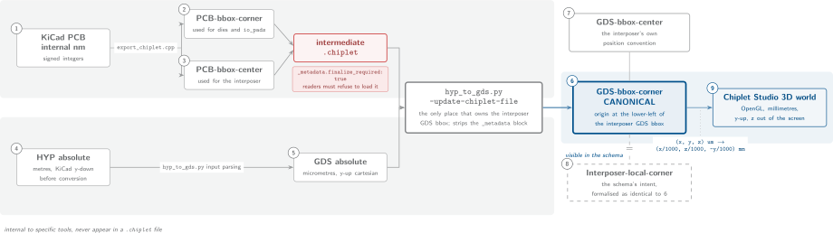
The nine coordinate frames in the toolchain, and where each conversion happens. Only frames 6 and 9 are visible outside the tools.
# |
Frame |
Origin |
Used by |
|---|---|---|---|
1 |
KiCad PCB internal nm |
KiCad’s signed integer internal units (nm) |
KiCad core; not exposed to |
2 |
PCB-bbox-corner |
Lower-left of |
KiCad |
3 |
PCB-bbox-center |
|
KiCad |
4 |
HYP absolute |
HyperLynx file native: metres, KiCad y-down convention before conversion |
|
5 |
GDS absolute |
GDS file native: micrometres, y-up cartesian |
KLayout; |
6 |
GDS-bbox-corner (canonical) |
Lower-left of the interposer GDS bbox |
This contract. Also |
7 |
GDS-bbox-center |
|
|
8 |
Interposer-local-corner |
The frame components mean to be in |
The schema’s intent, now formalised as identical to frame 6 |
9 |
Chiplet Studio 3D world |
OpenGL world: millimetres, y-up, z out of the screen |
|
Where to go next
The .chiplet assembly file for the schema these positions live in.
Pad to pillar alignment for the check that applies the transform on real designs.
Exporting the assembly for where the finalizer runs in the flow.
3Dblox interoperability for how the frame and orientation conventions translate on export.