
gds2kicad
gds2kicad, IHP-GmbH/gds2kicad, turns a die or chiplet GDSII into the KiCad
parts you need in order to design an interposer around it: a .kicad_mod
footprint, a .kicad_sym symbol, an editable pin list, and the netlist that
flows back into the assembly format.
It is the first tool in the flow, and From die GDS to KiCad walks through using it on a real die.
The problem it solves
KiCad cannot read GDS, so placing a die on an interposer in pcbnew requires a footprint, and the only information that footprint needs is already sitting in the die layout: where the bond pads are, how big they are, what shape they are, and what they are called.
The usual fallback is to redraw the pads by hand from a datasheet and type pin names in cell by cell: slow, error-prone in a way that only shows up after fabrication, and redone every time the die layout changes.
gds2kicad reads the pad geometry and the text labels straight out of the
layout, so the KiCad part matches the silicon by construction rather than by
transcription.
Installing
There is nothing to build. Run the scripts from the clone root. You need KLayout’s Python module to read GDS, and PyQt6 for the GUIs:
python3 -m venv venv && source venv/bin/activate
pip install -r requirements.txt    # PyQt6
pip install klayout
A system KLayout with its bindings on PYTHONPATH works too. In the container
none of this applies: run gds-to-kicad and the GUI opens.
Tip
Both converters can write themselves a small test GDS, which is the quickest way to check an install:
python3 gds_to_kicad.py --generate-test-gds
python3 gds_to_kicad.py tests/test_footprint.gds -o demo.kicad_mod
The result has three pads, numbered rather than named, because the fixture carries no text labels.
Telling it where the pads are
There is no PDK baked in, no --pdk flag and no PDK discovery. You say
explicitly which layer holds the pads, in one of three ways, in this order of
precedence:
Order |
How |
Example |
|---|---|---|
1 |
Raw GDS layer number, ignores the |
|
2 |
Layer name resolved through a KLayout |
|
3 |
Nothing, and the densest plausible pad layer is auto-detected |
(no flags) |
Pin names come from a separate text layer, selected the same way with
--text-layer NAME or --text-layer-number N/D, or auto-detected.
Note
Two things reliably cost people time.
The flag spelling differs between the two converters: gds_to_kicad.py
uses --layer, gds_to_kicad_symbol.py uses --pad-layer. The
*-layer-number flags are spelled the same in both.
More importantly, if you name the pad layer with --layer and say nothing
about text, gds_to_kicad.py emits numbered pads instead of named
ones, and it does so silently. Add --text-layer NAME, or --auto-text
to let it find the text layer itself. The symbol tool does not have this
problem because it derives TopMetal2.text from TopMetal2.drawing on
its own, which is why it has no --auto-text flag. When both tools
auto-detect the pad layer, both auto-detect the text layer too.
Auto-detection works on a clean chiplet GDS. On a full die it will happily return routing, fill and guard rings as “pads”. Inspect first:
python3 gds_to_kicad.py die.gds --scan-layers
python3 gds_to_kicad.py die.gds --list-layers --lyp-file pdks/sky130.lyp
The role of the .lyp
A KLayout layer-properties file is what maps a human-readable layer name onto a
GDS layer and datatype pair. gds2kicad uses it for nothing else: it does not
read design rules, it does not need a technology, and it does not care which
process the file describes. That is why any technology works, and why passing a
raw layer number bypasses the .lyp completely.
Four files ship under pdks/:
File |
Contents |
|---|---|
|
The default. A pads-only vocabulary: pad metal 205/0, pad text 205/25, outline 206/0. For closed chiplets that ship no layer file at all. |
|
The full IHP SG13G2 layer set. |
|
The full SkyWater sky130 layer set. |
|
SG13G2 upper metals through Bump, for interposer work. |
Drop any other technology’s .lyp into pdks/, or pass any path with
--lyp-file. IHP SG13G2 is what the tool is tested against most heavily, not
a requirement.
Die to footprint
python3 gds_to_kicad.py die.gds --lyp-file pdks/sg13g2.lyp \
    --layer TopMetal2.drawing --text-layer TopMetal2.text \
    -o die.kicad_mod
The converter reads the top cell, flattens it, collects box and polygon shapes from the pad layer, and names each pad from the nearest text label on the text layer.
Pad extraction
A rectangular pad becomes an ordinary smd rect pad. A non-rectangular pad
becomes an smd custom pad whose gr_poly primitive carries the real
vertices, expressed relative to the pad centre. This matters because octagonal
and chamfered pads are common on real silicon, and approximating them by their
bounding box would misreport the metal available for a bump landing.
Coordinates are converted GDS Y-up to KiCad Y-down by negating Y. Pad names are sanitised before being written, because both the cell name and the text labels come from a GDS file that the tool did not produce, and a stray quote or parenthesis would corrupt the S-expression.
--flip-chip mirrors X, so that a die mounting face-down on an interposer
reads as seen from the interposer side. It also changes the ORIENTATION
property written into the footprint from face_up to flip_chip, which is
the value the .chiplet exporter later keys its flip-chip handling on.
Traceability properties
Every generated footprint carries four properties recording where it came from:
Property |
Value |
|---|---|
|
Absolute path of the source GDS. |
|
Absolute path of the layer-properties file used. |
|
The pad layer, as name and as number, for example
|
|
|
These are not documentation. GDS_FILE is the field the KiCad fork’s
HyperLynx exporter emits on the device record, and the field the chiplet
exporter reads to fill in a die’s layout: entry. It is what lets the
downstream converter instantiate the real die layout instead of a placeholder
rectangle, without anyone typing a path into a board. ORIENTATION feeds the
flip-chip path in the same exporter. See KiCad ADK fork.
Note
The generated courtyard (F.CrtYd) is a rectangle over the pad bounding
box, not over the die outline. The chiplet exporter takes a component’s
width and height from the courtyard when one is present, so a die whose pads
sit well inside its edge will export with dimensions smaller than the
physical die. Draw the courtyard to the die outline in the footprint editor
if the assembly dimensions matter, which they do for the assembly placement
rules.
Die to symbol
python3 gds_to_kicad_symbol.py die.gds --lyp-file pdks/sg13g2.lyp \
    --pad-layer TopMetal2.drawing -o die.kicad_sym
Same pad and text extraction, emitted as a KiCad 6 or later .kicad_sym
library. Pins are placed automatically: pins whose names look like power or
ground go top and bottom, signals are distributed across the remaining sides so
the counts stay balanced. --symbol-name, --footprint-ref and
--max-text-distance (a DBU cutoff for matching a label to a pad) adjust the
result.
The pin list
Automatic classification is a starting point, not an answer. The pin list is the mechanism for correcting it, and it is the single source of truth for pin names, types and sides in the human-in-the-loop workflow.
python3 gds_to_kicad_symbol.py die.gds --extract-pins pins.json
# edit pins.json
python3 gds_to_kicad_symbol.py --from-pin-list pins.json -o die.kicad_sym
The rebuild step touches no GDS at all. Once a pin list exists it is the input, which means a naming correction survives a re-extraction only if you keep the file.
Each entry carries a name, a side (left, right, top,
bottom), a type (passive, input, output, bidirectional,
tri_state, power_in, power_out, unspecified) and the pad
geometry in database units, including the polygon vertices when the pad is not
rectangular. The file carries metadata alongside the pins: a format version, the
chiplet name, the source GDS, the .lyp, the pad layer, the text layers used
and a timestamp. Names such as <chiplet>_pins.json are the convention the
GUI and footprint_to_pinlist.py both default to.
The same file is what the Pin List Editor tab edits, what --pin-list
expects in the pad-review workflow below, and what bump_mirror.py in the
interposer PDK consumes to place bumps. Pin lists documents
the format.
Going the other way, footprint_to_pinlist.py pulls pad geometry out of one
or more .kicad_mod files into a pin list, converting KiCad millimetres back
to database units.
Curating pads by hand
This is the normal path for real silicon, not an advanced fallback.
A full die GDS is mostly routing, fill and guard rings, and no heuristic can tell those from bond pads. The workflow is to reduce the GDS to the pad layer plus labels, clean it up in KLayout where you can see what you are deleting, and then build from the result:
python3 gds_to_kicad.py die.gds --generate-pad-review review.gds
klayout -e -l pdks/sg13g2.lyp review.gds
# delete everything that is not a real pad, save
python3 gds_to_kicad.py --from-pad-review review.gds \
    --pin-list pins.json -o die.kicad_mod
--pin-list is required in the rebuild step. After a manual edit the shapes
in the file no longer correspond to the extraction that produced them, so the
pin list is the authoritative list of names; pads are matched to it by nearest
neighbour, and anything left unmatched is warned about rather than silently
numbered.
Database units
The converters do not assume a database unit. The scale factor comes from
layout.dbu of the file actually being read, resolved once per conversion and
threaded through every coordinate conversion. --dbu overrides it for a file
whose header is wrong.
The DBU is not a constant across the ecosystem: IHP SG13G2 layouts are conventionally 1 nm per unit, but a chiplet from another source may not be, and the wrong factor produces a footprint off by a power of ten that still looks plausible. When no layout is available the fallback is 1 DBU equals 1 nm, stated explicitly in the code.
Black-box chiplets
blackbox_chiplet.py handles the case where a chiplet comes from a commercial
or closed process and all you have is a pad map: names, centres and sizes, from
a datasheet. There is no layout and no layer file.
python3 blackbox_chiplet.py pads.json -o chiplet.gds
python3 blackbox_chiplet.py pads.csv  -o chiplet.gds --no-manifest
The input is JSON or CSV, chosen by extension. CSV is a header
name,x_um,y_um,w_um,h_um with one pad per row. JSON adds an optional
explicit die size (as width_um/height_um or as bbox_um) and a
chiplet_name. Pad x and y are centre coordinates. Without an
explicit die, the outline is derived from the pad extents plus a margin.
Pads, labels and outline are stamped on the ADK canonical generic layers, 205/0,
205/25 and 206/0, read from config/chiplet_pads.json under the discovered
ADK root with those values as a hardcoded fallback so the generator still runs
when the ADK is unreachable. Because those are exactly the layers
generic.lyp describes, the output feeds the converters above with no layer
flags at all.
Note
blackbox_chiplet.py is also a boundary-manifest producer. Alongside the
GDS it writes a <stem>.boundaries.json carrying the die outline as the
chiplet boundary, with schema adk-boundary-manifest version 1.0.0,
the same contract hyp_to_gds.py emits for a full assembly. That is what
allows the assembly DRC to check a standalone synthesised die, and it is why
the boundary is metadata rather than a layer: a stand-in GDS has no
fabrication layers to put it on. Suppress it with --no-manifest. See
Boundary manifest.
Interposer I/O pads
io_pads/ holds the other end of the interposer: the pads that connect the
assembly to the outside world.
python3 io_pads/generate_io_pad.py --io-class wire_bond --size 100x100
python3 io_pads/kicad_pcb_to_iopads.py design.kicad_pcb -o io_pads.json
generate_io_pad.py emits a parametric KiCad symbol and footprint tagged with
IO_CLASS and IO_PAD_SIZE_UM properties. IO_CLASS is the field the
chiplet exporter uses to tell an interposer I/O pad from a chiplet die, so the
tag is what puts the pad under the interposer’s io_pads rather than in the
component list. Only wire_bond is implemented; flipped_bump and
tsv_bump are reserved names and are rejected.
After routing, kicad_pcb_to_iopads.py walks the board, keeps the footprints
carrying an IO_CLASS, and writes their pad locations, sizes and nets to JSON,
converting millimetres to micrometres and negating Y for the GDS Y-up
convention. The export plugin performs the same extraction automatically; this
script is the standalone and override path.
Board back to chiplet netlist
python3 kicad_netlist_to_chiplet.py design.net --yaml nets.yaml --csv nets.csv
python3 kicad_netlist_to_chiplet.py design.net --inject board.chiplet --summary
Converts a KiCad S-expression netlist into chiplet-flow YAML or CSV, or injects
a netlist: section directly into an existing .chiplet. Nets are
classified as power, ground or signal by name. Footprints from the io_pads
library, or any reference prefix passed with --external-ref-prefix, are
flagged external: true. At least one of --yaml, --csv, --inject
or --summary is required.
The GUIs
unified_gui.py is the recommended entry point and drives the same engine as
the command line. It is a single window with five tabs, in workflow order:
Extract Pins, load a GDS and a
.lyp, optionally prepare a stripped pad-review GDS, extract the pin list.Pin List Editor, review and correct names, types and sides.
Symbol Designer, generate the
.kicad_symwith a live preview.Footprint Generator, generate the
.kicad_mod.History, a registry of past conversions.
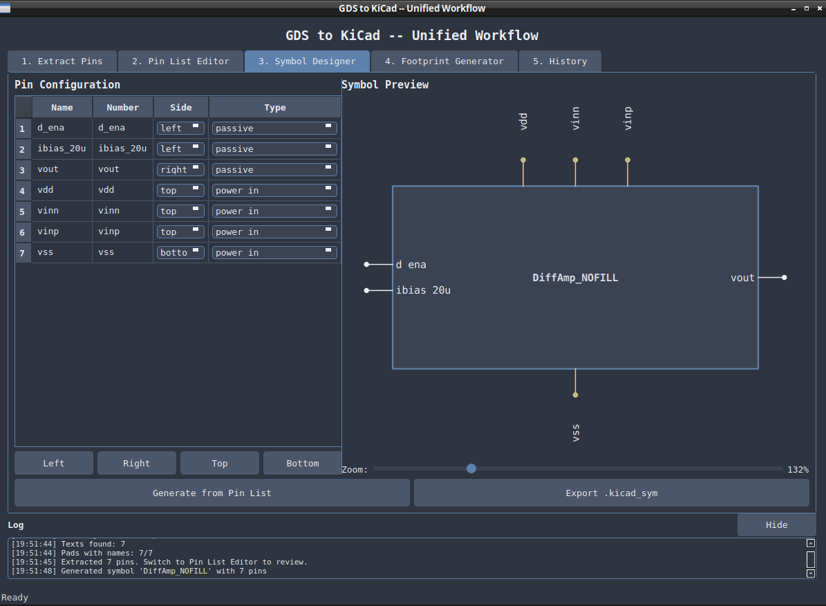
The Symbol Designer tab. The pin configuration table on the left is the pin list, one row per pad, with the side and the electrical type editable per pin; the preview on the right redraws as you change them, and Export .kicad_sym writes the library. The log records what the extraction found, here seven pads with seven names, and sends you to the Pin List Editor before anything is generated. That review step is the point: the tool proposes a classification, you confirm or correct it.
In the container this is what the gds-to-kicad command launches.
gds_to_kicad_gui.py and gds_to_kicad_symbol_gui.py remain as
single-purpose windows for footprints and symbols respectively. On a headless
machine set QT_QPA_PLATFORM=offscreen.
Where files are written
From the command line, generated files land in the current directory:
footprints under generated_kicad_footprint_files/, symbols under
generated_kicad_symbol_files/.
To control it |
Use |
|---|---|
An exact output path |
|
The per-design |
|
A different base directory |
the |
Defaulting to the working directory is what makes the tools usable inside the
container: the install directory is read-only for the non-root user and no home
directory is mounted, so only the shared /work tree persists.
The GUIs behave differently. Every export goes through a save dialog that
opens in the directory the GUI was launched from. Only the conversion history
registry is written under generated_kicad_symbol_files/.
One exception: io_pads/generate_io_pad.py writes back into the clone
(io_pads/kicad_symbols/ and io_pads/kicad_footprints/) unless you pass
--out-dir.
Tip
Every generated file is written atomically: the content goes to a sibling temporary file and is moved into place only once it is complete, so an interrupted or failing run leaves the previous artefact intact rather than a truncated one. Output is forced to UTF-8, and the file mode follows the umask rather than the owner-only default, which is what keeps generated files readable across the container’s shared mount.
Troubleshooting
Symptom |
Cause |
|---|---|
|
|
Qt “xcb platform plugin” error on Linux |
Missing Qt system libraries, or use |
Footprint pads come out numbered, not named |
|
Thousands of pads, huge output file |
Auto-detection grabbed routing or fill. Use the pad-review workflow. |
|
The examples use paths relative to the clone root. Run from there, or
pass an absolute |