
Generating the assembly GDS
The KiCad export of Exporting the assembly leaves you with a HyperLynx .hyp
netlist and an intermediate .chiplet file. Neither is fabrication geometry:
the .hyp describes traces as centre lines with widths, vias as padstack
indices, and dies as position-only anchors pointing at external GDS files.
hyp_to_gds.py, the worker of the IHP-GmbH/Chiplets-KiCad-Plugin repository, turns that
description into GDS layouts on real process layers, generates the attachment
structures, and writes the sidecar manifests the assembly checks consume.
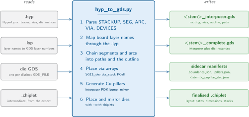
The converter’s input and output contract. Everything on the left is read, everything on the right is written, and the numbered stages are the order in which the geometry is built.
In the ADK-Tools image the worker is on the path as hyp-to-gds. Outside the
image it is hyp_to_gds.py at the root of the plugin checkout, run with a
Python interpreter that has the klayout module installed.
Note
The KiCad Chiplet Export plugin runs this converter for you and builds its
argument list from the export options. Run it by hand when you are
scripting the flow, when
you want to regenerate the GDS after editing the .hyp, or when you are
debugging what the plugin produced.
What the converter consumes
hyp_to_gds.py takes one positional argument, the .hyp file, and reads
these inputs:
.hyp(required)Board geometry from KiCad. The converter parses the
STACKUPsection (layer order, top to bottom),PADSTACKdefinitions, per-net trace segments and arcs, via instances, theBOARDperimeter (the KiCadEdge.Cutsoutline), and theDEVICESsection, where each chiplet appears with a reference designator, a layer, aGDS_FILEpath, a rotation, and the position of the KiCad footprint’s own anchor (with Y negated so it shares the coordinate system of the traces). The converter takes that position as given; it computes no centroid.- A KLayout layer properties file (
--lyp) The name-to-number mapping. Board copper layers are matched by name against the
.lypentries, soTopMetal2in the board stackup becomes GDS layer 134/0 because the interposer technology says so. By default the converter resolves the interposer PDK’s canonicalintm4tm2.lypthrough the discovery chain (INTERPOSER_PDK_ROOT, then a sibling checkout); the layer table belongs to the PDK, and there is no plugin-local copy.- Die layouts
One GDS per distinct
GDS_FILEreferenced by the.hyp, read only when--with-chipletsis given.- Optional sidecars
--tech-jsonfor the interposer via parameters,--pad-locationsfor per-die pin lists that drive Cu-pillar generation,--io-padsfor external I/O pad geometry,--cupillar-gdsto merge pillars generated elsewhere, and--update-chiplet-fileto finalise the intermediate.chiplet.
Every path argument may use ${VAR} references to the ecosystem discovery
variables, for example
${INTERPOSER_PDK_ROOT}/libs.tech/klayout/tech/intm4tm2.lyp. Writers copy
those strings verbatim; the converter expands them on read, falling back to a
sibling-checkout walk and then failing loudly with the variable name. See
Environment and path discovery.
What it produces
Artefact |
Contents |
|---|---|
|
The interposer alone: routing, vias, the board outline on
|
|
The full assembly: the interposer plus every die instance, placed and
mirrored. Written only with |
|
One mechanical boundary polygon per placed chiplet. Written next to every GDS the converter emits. See Boundary manifest. |
|
The as-drawn Cu-pillar and bump centres. Written whenever the bump generation path ran. See Pillar manifest. |
|
The per-die Cu-pillar DRC report from the interposer PDK’s bump validator, aggregated across dies. |
The finalised |
Rewritten in place with |
The output paths default to <hyp-stem>_interposer.gds and
<hyp-stem>_complete.gds next to the .hyp; -o and
--complete-output override them. The top cell name defaults to
INTERPOSER and is set with -c.
Running it
A minimal interposer-only conversion:
hyp-to-gds two_die_interposer.hyp -o layout/two_die_interposer_interposer.gds
The full form the export pipeline uses, producing both GDS files and finalising
the .chiplet:
hyp-to-gds two_die_interposer.hyp \
    -o layout/two_die_interposer_interposer.gds \
    -c INTERPOSER \
    --with-chiplets \
    --complete-output layout/two_die_interposer_complete.gds \
    --update-chiplet-file two_die_interposer.chiplet \
    --die-connections U1=cupillar_opt1,U2=vendorx_microbump \
    --die-thicknesses U1=750,U2=750 \
    --pad-locations U1=../chiplets/metal_test_chiplet.pins.json,U2=../chiplets/metal_test_chiplet.pins.json \
    --io-pads io_pads.json
From KiCad routing to fabrication geometry
Copper layers must be named after the process metals
The single most common way to get an empty-looking GDS is to route on KiCad’s
default copper layer names. The converter maps a board layer to a GDS layer by
looking its name up in the .lyp, so F.Cu maps to nothing at all. Rename
the copper layers in Board Setup > Board Editor Layers so they read
TopMetal2, TopMetal1, Metal5 and Metal4, or start from the
template board the interposer PDK ships at
libs.tech/kicad/interposer_template.kicad_pcb, which has the renames
already applied. The converter’s own error message points at that same file,
resolved through INTERPOSER_PDK_ROOT.
The converter accounts for what it dropped. If more than half of the trace
elements sit on layers the .lyp does not map, the conversion aborts and
prints the unmapped board layers next to the list of drawing layers the PDK
does offer. Below that threshold the strays are tolerated with an aggregate
warning. The reasoning is that a GDS missing most of its routing still looks
like a valid layout, and nothing downstream can tell that traces were supposed
to be there.
Traces, arcs and the outline
Segments and arcs of the same net, layer and width are chained end to end into
continuous paths before they are written, so a polyline routed as ten KiCad
segments becomes one GDS path with clean corners rather than ten overlapping
rectangles. Arcs are flattened into 16 chords. Coordinates are converted from the
.hyp unit system (inches or metres) to micrometres on a 1 nm database unit,
with the Y reflection that the GDS convention requires.
The BOARD perimeter segments are chained into closed loops and drawn on
prBoundary (235/0 in the current IntM4TM2 layer map; layouts generated
before the July 2026 layer-map parity migration carry it on 189/0). This is
all or nothing: if any segment fails to chain into a closed loop, nothing is
drawn and the converter says so, because a partial outline understates the
board extent and would silently shrink the interposer dimensions written into
the .chiplet.
After writing the interposer GDS the converter compares the drawn-geometry bounding box against the outline and warns per side when copper or a die sticks out. That is an early, cheap version of the containment check: KiCad’s own DRC flags an off-board footprint at design time, and this catches the same mistake at the GDS.
Vias come from the base PDK’s own PCells
A .hyp via is a padstack index and a coordinate. Turning that into
fabricable geometry means choosing a via array that approximates the padstack
pad size, drawing the cuts on every via level between the two metals, and
drawing a landing pad on every metal of the span with the correct enclosure.
The converter does not reimplement that. It registers the SG13G2 PCell library
in its own process, the same thing the PDK’s autorun.lym does inside a
KLayout session, and then instantiates the PDK’s via_stack PCell from the
SG13_dev library with the computed row and column counts. Discovery follows
PDK_ROOT first, then a sibling IHP-Open-PDK checkout. Because the
library is technology bound, the converter also registers the sg13g2
technology and binds its layout to it; without that binding the cell lookup
returns nothing even with the library loaded.
This matters more than it looks. The via ladder, the cut sizes, the separations and the metal enclosures are process rules that live in the base PDK and change with it. Placing the PDK’s own parameterised cell means the assembly GDS carries exactly the geometry a designer would have drawn by hand in that process, and it keeps tracking the PDK when those numbers move. A hand-rolled approximation is a second implementation of somebody else’s rules, and it drifts silently.
When the PDK is not reachable the converter degrades rather than failing: it
prints that PCells are unavailable and draws the vias from plain rectangles.
The fallback is deliberately not a single oversized box. It uses the same array
formula as the PCell path, draws an n by n array of PDK-sized cuts per via
level, and gives every metal of the span a landing pad enclosing its adjacent
arrays by the PDK enclosure, with the numbers taken from
interposer_tech_default.json when --tech-json supplies it. Cuts without
a landing pad would be enclosure violations, and a metal transition that no via
pair covers is refused outright instead of drawing floating landing pads.
Tip
The ADK-Tools image bakes PDK_ROOT at the SG13G2 KLayout slice, so
hyp-to-gds always takes the PCell path there. Outside the image, check
the converter’s own log line: it announces which path it took before it
starts placing vias.
Cu pillars and bumps
Attachment structures are generated, not routed. Give the converter a per-die
pin list with --pad-locations REF=FILE and a connection method, either
assembly-wide with --connection-type or per die with --die-connections
REF=METHOD, and it places one pillar per pad.
The geometry does not come from the plugin either. The converter imports
bump_mirror from the interposer PDK
(libs.tech/klayout/python/bump_mirror.py) for the fabrication pads and the
Cu-pillar rule checks, and reads the interconnect PDK manifest for the method’s
3D body layers, body diameter, passivation opening and pitch rules. Each method
in use gets its own generator and its own parameter set, so an assembly can mix
methods: in the reference design U1 is attached with cupillar_opt1
(44 um body, 75 um pitch, 40 um spacing) and U2 with vendorx_microbump
(40 um body, 50 um pitch, 15 um spacing), and each die’s pillars are drawn and
checked against its own numbers.
A method’s declared pitch_rules in the interconnect manifest take precedence
over the body-diameter lookup table. This is what lets a vendor method with an
out-of-table body diameter be checked at its real pitch rather than at the
generic defaults.
For each die the converter computes the bump locations from the pin list and the
die placement, runs a collision auto-resolve pass, validates the result against
the method’s rules, and records what it actually drew. Bumps the auto-resolve
moved are marked in the pillar manifest together with the shift magnitude, so a
later pad-to-pillar check can tell an intentional shift from a real
misalignment. Residual violations are reported and the run continues, with the
complete report persisted to <stem>_cupillar_drc.json.
Why a missing interposer PDK is fatal here
When at least one die requests a connection method and bump_mirror cannot
be imported, the converter refuses to write anything and tells you to set
INTERPOSER_PDK_ROOT.
This is the opposite policy from the via PCells, and the asymmetry is deliberate. A missing via PCell degrades to geometry that is still there and still approximately right. A missing pillar generator produces a complete looking GDS with no attachment structures at all, and no downstream check can flag geometry that was never drawn: the assembly DRC checks the pads that exist, and finds none to complain about. The failure would surface at assembly, not in the flow. So the converter treats an unreachable interposer PDK as a hard error whenever pillars were requested.
The same reasoning drives the other hard stops: --with-chiplets with zero
die GDS files successfully loaded refuses to emit a die-less complete GDS, and a
.chiplet that could not be finalised reports failure rather than exiting
zero on a file Chiplet Studio will reject.
Flip-chip placement
A die attached by a body-bearing method is mounted face down. In the assembly GDS that is realised as a mirror in X, applied to the die artwork before rotation.
The converter does not place a mirrored instance. It instantiates the imported die template with the mirror transform into a wrapper cell and flattens that wrapper, so the mirrored artwork exists as real geometry on each layer. The reason is downstream consumption: EM and thermal tools, and anything else that walks shapes per layer, see the correct polygons without having to interpret instance-level mirroring. The die template itself is kept, so a second instance of the same die reuses it.
What the GDS does not capture is the z inversion of the die’s BEOL stack.
Mirroring in X puts the artwork in the right place in plan view; the fact that
the die’s top metal now faces down belongs to the stackup, and is handled by
the .chiplet orientation and the stackup descriptions the 3D tools read.
Which dies are flipped is decided from two sources, unioned. The primary signal
is the die’s connection method: a method with a body diameter in the
interconnect manifest implies flip-chip, so the orientation does not depend on a
.chiplet being present. When --update-chiplet-file is in play, the
.chiplet components are read as well and any die declaring
orientation: flip_chip or carrying a connection is added. An orientation
token that is neither face_up nor flip_chip is a hard error: the frame
contract defines only those two, and silently treating a typo (or the plausible
looking face_down) as face up would flip a die the wrong way with no
diagnostic.
Sidecars written alongside the GDS
Every write emits its manifests next to the layout it just wrote, which
means both the interposer GDS and the complete GDS get their own set.
Boundary manifest
<gds-stem>.boundaries.json carries one polygon per placed chiplet, each with
its instance, its source_die and the transform that placed it
(origin, rotation, mirror, magnification). polygon_dbu is authoritative and
polygon_um is provenance. The manifest also records the database unit, the
top cell and a SHA-256 of the GDS it describes. It is always written, even with
zero boundaries, so a manifest is always present beside the layout.
The boundary deliberately lives outside any fabrication layer namespace. Earlier
versions stamped it on the exchange0 layer (190/0), a real IHP SG13G2
fabrication layer; nothing emits 190/0 any more. The assembly DRC runner
auto-discovers the manifest next to the GDS; see Running the assembly DRC.
Pillar manifest
<gds-stem>.pillars.json records the as-drawn pillar centres, per die and per
pin name, with the method and body diameter, in the canonical GDS bounding-box
corner frame that .chiplet positions and I/O pads also use. The frame origin
is captured at the first manifest write, before die instances are merged in, and
reused for the complete GDS so both sidecars share one frame. See
Coordinate frames.
The manifest is written only when the bump generation path actually ran, and it
distinguishes two cases that would otherwise look alike: no manifest at all
means the bump path never ran, while a manifest with an empty pillars array
means it ran and drew nothing.
Optional boundary annotation
--annotate-boundaries additionally paints each boundary polygon, plus an
instance label, onto a viewer-only annotation layer, 1000/0 by default and
overridable with --boundary-viz-layer. It is off by default, no DRC rule
reads that layer, and the converter refuses an annotation layer that collides
with a fabrication layer, because the painter clears the layer before drawing
and would wipe real geometry.
For inspecting boundaries you generally do not want this at all: the ADK ships a viewer that renders the same manifest as KLayout markers without touching the GDS. See Viewing and inspecting.
After the conversion
The GDS and its sidecars are the input to the assembly checks. Run the KLayout
assembly DRC on the complete GDS, and the manifest-level pad-to-pillar check on
the .chiplet plus the pillar manifest. Verification stages
explains what each stage proves and in what order to run them.