
Interposer PDK (OpenIntM4TM2)
OpenIntM4TM2 is the KLayout PDK for the IHP 130 nm IntM4TM2 aluminium back-end interposer. It is the substrate the reference flow assembles onto, and from the ADK’s point of view it is simply one more PDK reached through an adapter: the ADK never reads a layer number from it.
Repository: IHP-GmbH/OpenIntM4TM2. Apache-2.0.
Warning
OpenIntM4TM2 is a Preview Release, and its own README states that DRC and LVS are still work in progress. The process has been fabricated several times at IHP, which is a statement about the maturity of the process, not about any complete assembly built on it, and not a claim that these rule decks are signed off.
The process
IntM4TM2 is a passive interposer technology derived from the IHP SG13G2 130 nm BiCMOS process. Every front-end device layer is removed. What remains is the aluminium back-end redistribution stack, Metal4 through TopMetal2, plus the passive devices and the assembly-facing features built on top of it: MIM capacitors, thin-film resistors, passivation and pad openings, the edge seal, and localized backside etch (LBE).
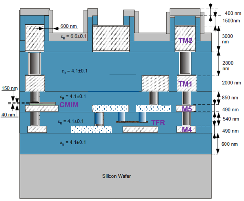
Cross-section of the IntM4TM2 interposer: four aluminium metals (Metal4, Metal5, TopMetal1, TopMetal2) on a high-resistivity silicon carrier, with the thin-film resistor between Metal4 and Metal5, the MIM capacitor between Metal5 and TopMetal1, and the top passivation. The dielectric constants and layer thicknesses are the typical-corner values published in the PDK extraction stackup. Cu-pillar bumps are interconnect elements attached into the pad openings, not part of the fabrication stack.
Three consequences follow, and they explain most of the PDK.
Metal4 is the lowest routing metal. There is no Metal1 to Metal3 and no transistor underneath. The M4 to TM2 block keeps the SG13G2 layer thicknesses and inter-metal spacings unchanged, because they are identical in the base process, and is shifted down by 3.42 um so Metal4 starts about 0.64 um above the carrier surface.
The routing budget is four metals. Two thin (Metal4, Metal5) and two thick (TopMetal1, TopMetal2). Anything the assembly needs to route, it routes there.
The fab side owns the pad openings, not the bumps. The interposer fabricates the under-bump openings. What is attached into them is a separate vendor axis, which is why the bumping method lives in a different repository. See Interconnect PDK.
The metal stack
The vertical stack, taken from the electromagnetic and extraction stackups that ship with the PDK, with z = 0 at the carrier top surface:
Layer |
GDS layer |
z min (um) |
z max (um) |
Thickness (um) |
|---|---|---|---|---|
TopMetal2 |
134 |
7.8103 |
10.8103 |
3.000 |
TopVia2 |
133 |
5.0103 |
7.8103 |
2.800 |
TopMetal1 |
126 |
3.0103 |
5.0103 |
2.000 |
TopVia1 |
125 |
2.1600 |
3.0103 |
0.850 |
Metal5 |
67 |
1.6700 |
2.1600 |
0.490 |
Via4 |
66 |
1.1300 |
1.6700 |
0.540 |
Metal4 |
50 |
0.6400 |
1.1300 |
0.490 |
Above TopMetal2 sit 1.5 um of oxide and 0.4 um of SiN passivation, so the total build-up from the carrier surface to the top of the passivation is about 12.71 um. The inter-metal gaps reproduce the module specification exactly: Metal4 to Metal5 is 0.54 um, Metal5 to TopMetal1 is 0.85 um, TopMetal1 to TopMetal2 is 2.80 um.
Connectivity for net tracing is declared in the technology file as three
stacks: Metal4-Via4-Metal5, Metal5-TopVia1-TopMetal1 and
TopMetal1-TopVia2-TopMetal2.
The KLayout technology
Install it in KLayout with Tools > Manage Technologies > Import Technology,
pointing at libs.tech/klayout/tech/intm4tm2.lyt. The layer properties and the
stream layer mapping are picked up from the technology file automatically.
File |
Purpose |
|---|---|
|
The technology itself. Name |
|
Layer properties: colours, fill patterns, and the GDS layer/datatype assignment for every entry. |
|
The canonical layer list, one |
|
EDI stream layer mapping for the backend metals, vias and pad layers.
|
How many layers
Three different counts are all defensible, so say which one you mean. The
.lyp is an
XML document with 224 <name> elements in total, but
they are not all layers: 54 are custom dither patterns and 12 are custom line
styles. The layer entries proper are the 158
<properties> elements, each carrying exactly one <name> and one
<source>, and those match the rows of intm4tm2_layers.txt one for one.
Those entries cover |interposer-layer-names| distinct layer names: Metal4, Via4,
Metal5, TopVia1, TopMetal1, TopVia2, TopMetal2, MIM,
Vmim, Passiv, dfpad, Recog, EdgeSeal, LBE,
ThinFilmRes, IND, NoMetFiller, NoRCX, BackMetal1,
BackPassiv, IC, TEXT, prBoundary, instance and
Exchange0 through Exchange4. The remainder is the purpose
axis, 35 distinct purposes in all. Most entries carry one of the routine ones,
drawing, label, pin, net, boundary, filler, nofill,
slit, text, mask, OPC, noqrc, res, iprobe or
diffprb. The rest are recognition and extraction purposes carried over from
SG13G2, among them esd, diode, mom, otp, tsv, pcm and
the ten NoRCX inter-layer purposes from m4m5 to tm2sub. Two are new
to assembly: pillar (datatype 35) and sbump (datatype 36).
Note
The pillar and sbump purposes are the ones that matter to assembly.
A Cu-pillar attachment point is the intersection of Passiv:pillar (9/35)
and dfpad:pillar (41/35); the solder-bump equivalent uses datatype 36.
That intersection is exactly what the ADK’s intm4tm2 interposer adapter
exposes as the abstract chiplet_attachment_input, and it is the whole
content of the adapter file. See Adapter contract.
Tip
libs.tech/klayout/intm4tm2_tests/test_layer_parity.py asserts that the
.lyp and intm4tm2_layers.txt agree exactly. If you add a layer, add
it to both, or the test tells you which one you forgot.
DRC
The runset is libs.tech/klayout/tech/drc/intm4tm2.drc, driven by a Python
CLI wrapper rather than invoked directly:
python3 libs.tech/klayout/tech/drc/run_drc.py --path <layout.gds> --topcell <cell>
The runset always loads layers_def.drc first, then concatenates the selected
rule decks and evaluates the whole thing as a single Ruby string. That single
eval is deliberate: Ruby’s load runs in main scope and separate eval
calls do not share locals, so concatenating is what lets every deck see the same
layer definitions, the same drc_rules hash and the same logger.
The decks
Twenty decks are selectable. Nineteen of them run when you pass no --deck;
density is skipped by default.
Deck |
Rule table |
Checks |
|---|---|---|
|
3.1 |
Vertices on the manufacturing grid, circles exempt |
|
3.2 |
Allowed edge angles (vias 90, metals 45 and 90) and acute corners |
|
5.17 |
Metal4 and Metal5 width, space, wide-line space, 45 degree bends |
|
5.18 |
Metal4 and Metal5 filler width and space to drawn metal |
|
5.20 |
Via4 size, spacing, array spacing, metal enclosure and endcap |
|
5.21 |
TopVia1 size, spacing, enclosures |
|
5.22 |
TopMetal1 width and space |
|
5.23 |
TopMetal1 filler width and space |
|
5.24 |
TopVia2 size, spacing, enclosures |
|
5.25 |
TopMetal2 width, space, recommended wide-line space |
|
5.26 |
TopMetal2 filler width and space |
|
5.27 |
Passivation opening width, space, enclosure |
|
6.9 |
Pad recognition consistency, metal exit length, pad to seal ring |
|
6.9.2 |
Cu-pillar opening size, space, pitch, TopMetal2 enclosure, shape |
|
6.9.1 |
Solder-bump opening size, space, pitch, enclosure, shape |
|
6.10 |
Seal ring integrity, corners, uniqueness, outside structures |
|
6.11 |
MIM width, space, enclosures, per-device min and max area, via coverage, total area |
|
7.3 |
Slit size and coverage on wide metal plates |
|
9.1 |
Local back etch size, spacing, keep-outs |
|
(opt-in) |
Global and local metal, slit and LBE density |
python3 tech/drc/run_drc.py --path <layout.gds>                        # all default decks
python3 tech/drc/run_drc.py --path <layout.gds> --deck pad             # one deck
python3 tech/drc/run_drc.py --path <layout.gds> --deck lbe --deck pad  # two decks, merged
python3 tech/drc/run_drc.py --path <layout.gds> --mp 5                 # 5 decks in parallel
python3 tech/drc/run_drc.py --path <layout.gds> --density --density_sanity
Other options are --topcell (auto-detected when omitted), --run_dir
(default: a timestamped subdirectory), --threads (per invocation, default 4)
and --run_mode (tiling, deep or flat, default tiling).
--mp defaults to 1, which is a single KLayout invocation evaluating every
default deck. Raising it changes the execution strategy as well as the worker
count: the decks are expanded and run one invocation each, which costs a layout
load per deck and buys wall-clock time on a many-core machine.
Note
density is opt-in because it carries global minimum density rules.
Those are meaningless on a partial layout or a unit test fixture and would
report a violation on every one of them. Its DEN.BND.* boundary sanity
rules are separately gated behind --density_sanity.
Warning
Do not read these rule values as a statement of what IHP will accept for a
tapeout. They are derived from the SG13G2 layout rules revision the JSON
records, adapted to a stack that has no front end, and some adaptations are
documented in the decks themselves. The pad deck, for instance, notes
that the SG13G2 source checks pad-to-seal-ring separation against the
Activ component of the seal ring; the interposer has no Activ, so the
metal seal ring is substituted.
Rule values
Every numeric rule value is read at run time from
tech/drc/rule_decks/interposer_tech_default.json, never hardcoded in a deck.
The file records the revision it is based on, and a deck that asks for a missing
key raises rather than silently defaulting:
def fetch_rule(rules, key)
  unless rules.is_a?(Hash) && rules.key?(key) && !rules[key].nil?
    raise "DRC rule '#{key}' missing in interposer_tech_default.json"
  end
  Float(rules[key])
end
The JSON ships the Cu-pillar values for Table 6.1 Option 1 (35 um opening). Switching to Option 2 or Option 3 means editing three keys, and the file says so in its own description:
Option |
Opening (um) |
|
|
|
|---|---|---|---|---|
1 |
35 |
35 |
40 |
75 |
2 |
40 |
40 |
40 |
80 |
3 |
45 |
45 |
50 |
95 |
Padc_c (7.5 um TopMetal2 enclosure) and Padc_d (30 um to the edge seal)
are the same for all three.
Note
Two of these rules are checked here even though the source layout rules mark
them “not checked during DRC”: Padc.e (pitch) and Padc.f (shape).
They are checked anyway as safeguards for the assembly flow. KLayout has no
native pitch check, so pitch is converted to a spacing as
min_space = min_pitch - min_pad_size, which is conservative for pads
larger than Padc_a. Several Cu-pillar rules also carry a 10 nm tolerance,
because a circle drawn exactly at the minimum measures a few nanometres short
after 256-point approximation and nanometre-grid snapping.
Testing
The rule decks have their own regressions, following the IHP testing/
convention: one testcase GDS per rule table with a *_viol and a *_clean
top cell, compared against golden expectations.
python3 tech/drc/testing/run_regression.py                  # all tables
python3 tech/drc/testing/run_regression.py --table copperpillar
Tip
Each testcase GDS has a gen_<table>_testcase.py beside it. Regenerate
rather than hand-editing the GDS, otherwise the next regeneration silently
reverts your edit.
LVS
tech/lvs/intm4tm2.lvs, driven by tech/lvs/run_lvs.py, extracts
metal-stack connectivity, names nets from text labels, and reports opens and
shorts. MIM capacitors are extracted as cap_cmim devices: bottom plate on
Metal5, top plate on TopMetal1 through the Vmim via array, with parameters
w, l, A, P and parallel multiplicity m.
python3 tech/lvs/run_lvs.py --layout=<layout.gds>                       # connectivity only
python3 tech/lvs/run_lvs.py --layout=<layout.gds> --netlist=<ref.spice> # with compare
A reference netlist is optional. When one is given, KLayout’s netlist compare runs in strict port mode in addition to the label checks, so a device terminal left on a floating net (a capacitor without its via, for example) fails the compare rather than passing quietly.
The scope is one interposer layout against one reference netlist, in the interposer technology, with the interposer’s own device set. That is level 2 of the three levels of LVS in a 2.5D assembly, and it is ordinary PDK LVS. A clean result here says nothing about level 3, whether the dies are connected to each other as the system netlist declares. That level is within the ADK’s scope and no implementation of it is part of this preview release. What the ADK is sets out all three levels and both axes of assembly verification.
The PCell library
libs.tech/klayout/python/intm4tm2_pycell_lib registers a pya.Library
named IntM4TM2 bound to the intm4tm2 technology. The technology macro
tech/pymacros/autorun.lym bootstraps sys.path and imports it, the same
way the SG13G2 open PDK serves its own pycell library.
Cell |
Key parameters |
Output |
|---|---|---|
|
|
TopMetal2 134/0, |
|
|
MIM 36/0 plate, Metal5 67/0 bottom plate, TopMetal1 126/0 top plate,
|
|
|
Top-metal pad with a |
Note
bondpad and CuPillarPad are deliberate complements. bondpad
draws the plain dfpad purpose so the bond-pad rule table applies to it;
CuPillarPad rides the pillar purpose (datatype 35) precisely to avoid
those rules and to pick up the Cu-pillar table instead.
Cu-pillar generation
libs.tech/klayout/python/bump_mirror.py is the standalone Cu-pillar pad
generator. It takes pin lists, places and mirrors the pads onto the interposer,
DRC pre-validates them against the interposer rules, and only then writes GDS.
# Validate only, no GDS output:
python3 python/bump_mirror.py --pins U1=pins_u1.json U2=pins_u2.json \
    --chiplet design.chiplet --validate-only --report report.json

# Generate the Cu-pillar GDS:
python3 python/bump_mirror.py --pins U1=pins_u1.json --position U1=1000,2000 \
    -o cupillars.gds
Positions come either from --position REF=X,Y (with --rotation REF=DEG)
or from a .chiplet file via --chiplet; the two are mutually exclusive and
one is required. --diameter and --enclosure override the passivation
opening and the TopMetal2 enclosure. --report FILE writes a JSON validation
report.
Auto-resolve is on by default: when the placement produces a DRC collision, the
generator conservatively shifts pillars within a per-pillar budget
(--max-displacement, default 10 um) rather than failing. --no-auto-resolve
turns that off and fails on any violation instead;
--auto-resolve-best-effort emits GDS with warnings even when auto-resolve
does not converge.
Two properties of this generator are worth understanding.
The PCell is the single source of the pad geometry. CuPillarGenerator is
a thin placer that instantiates the CuPillarPad PCell and flattens it into
the output GDS. It does not redraw the pad. A parity test pins the placed output
to a directly instantiated PCell, per-layer XOR empty, for every Table 6.1
option. Parameter values in the assembly flow come from the interconnect PDK
manifest, not from this file.
It refuses to draw bodies it does not own. The 3D pillar and bump volumes
belong to the interconnect PDK. bump_mirror.py resolves that PDK through
$INTERCONNECT_PDK_ROOT first, then a sibling checkout named
interconnect_pdk or IHP-Interconnect-IntM4TM2. If neither resolves it
raises RuntimeError("interconnect_pdk not found") rather than emitting pads
without their bodies, which would look correct and be silently incomplete. The
failure is raised when a pad cell is built, so --validate-only still works
without the interconnect PDK on disk: the validator is coordinate arithmetic
against the interposer’s own Padc_b and Padc_e, with no GDS involved.
In the KiCad flow, hyp_to_gds uses this same module. It either merges a
pre-generated GDS passed with --cupillar-gds, or imports bump_mirror
directly and generates the pillars during export; without a resolvable
INTERPOSER_PDK_ROOT it refuses to emit a complete assembly GDS rather than
emitting one without pillars. See Generating the assembly GDS.
The KiCad side
Interposer assemblies are drawn as KiCad boards, so the PDK ships the KiCad-side
technology as well, under libs.tech/kicad/.
The board template
interposer_template.kicad_pcb is a four-copper-layer board whose copper
layers are already renamed after the PDK metals:
KiCad layer |
PDK metal |
Notes |
|---|---|---|
|
|
Top thick metal, carries the pad openings |
|
|
Thick metal |
|
|
Thin metal |
|
|
Lowest routing metal |
The reason to start from the template is mechanical: the HYP-to-GDS exporter maps
board copper to PDK metals by name. A board that keeps the default KiCad
names leaves its routing on layers the PDK does not recognise. When most of the
routing lands on unmapped layers the exporter aborts and points back at the
template; when only some of it does it warns and continues. You can reproduce the
renames on an existing board through Board Setup > Board Editor Layers
instead.
Three board text variables tie the board to the PDKs. The template ships none of them populated, on purpose.
Variable |
Meaning |
|---|---|
|
Path to the layer properties file. Use the portable form
|
|
The ADK interposer adapter id used by the assembly DRC. Defaults to
|
|
Optional interconnect method id, validated against the interconnect
PDK manifest at export time. Per-die overrides go in a |
Draw the interposer outline on Edge.Cuts: the exporter derives the interposer
dimensions from its bounding box and warns about components placed outside it.
The template’s example routing (a small mesh on Metal5, a few traces, four
vias) is there as a reference and is meant to be deleted.
Device footprints and symbols
libs.tech/kicad/footprints/intm4tm2.pretty holds the MIM capacitor family.
The footprints are real-size: each mirrors the plate geometry of the KLayout
PCell rather than using a symbolic land pattern, so the copper drawn on the board
is the same size as the capacitor drawn in the layout. For a plate w by
l (um), the MINUS plate on Metal5 is the outer (w + 1.2) x (l + 1.2)
rectangle and the PLUS plate on TopMetal1 is the inner rectangle from the PCell
via array, concentric with it.
Because those two plates are on the inner copper layers, pad 1 lands on
In1.Cu (TopMetal1) and pad 2 on In2.Cu (Metal5). Routing to a capacitor
therefore happens on the inner metals, not on F.Cu or B.Cu. This is
correct for the interposer stack and surprises people used to ordinary SMD parts.
The family is keyed by round capacitance rather than by round plate dimensions,
from CMIM_10fF to CMIM_5pF, with each member’s w = l being the
grid-snapped square-cap solution for its nominal value (every member lands within
about 0.1 percent of nominal). scripts/cmim_footprint_gen.py generates them,
and can solve an arbitrary target on demand:
python3 scripts/cmim_footprint_gen.py --cap 250f --out my_cmim.kicad_mod
python3 scripts/cmim_footprint_gen.py --w 12u --l 8u --out my_cmim.kicad_mod
python3 scripts/cmim_footprint_gen.py --family
The generator re-implements the PCell plate maths from the same
intm4tm2_tech.json the PCell reads, so it has no KLayout dependency. The
duplication is not allowed to drift: a test regenerates the real PCell headlessly
and asserts each footprint’s pad sizes equal the PCell’s Metal5 and TopMetal1
bounding boxes within 2 nm.
The schematic side is symbols/cap_cmim.kicad_sym, a hybrid set: one generic
cap_cmim (edit w and l for any value) plus nine value-keyed derived
symbols. The reason the values are pre-baked is that KiCad cannot back-solve
capacitance live, so there is no way to type “100 fF” and have the editor compute
the plate size. The netlist still carries w, l and m, never a
capacitance number; the displayed capacitance is informational.
What INTERPOSER_PDK_ROOT provides
Other tools in the flow do not hardcode any of the above. They locate this
repository through INTERPOSER_PDK_ROOT (or a sibling checkout named
interposer or OpenIntM4TM2, validated by the presence of
libs.tech/klayout) and read from it:
Consumer |
What it takes |
|---|---|
|
|
Chiplet export plugin |
The same root, resolved for the export dialog and forwarded to the orchestrator |
Chiplet Studio |
|
ADK assembly DRC |
Nothing directly. It reaches the interposer only through the
|
The last row is the important one. See Architecture.
Note
The assembly deck used to live in this repository and was promoted out of
it into the ADK. run_drc.py still recognises the name and redirects you to
adk/klayout/drc/run_drc.py --interposer-adapter <name>. See
Running the assembly DRC.
Simulation and extraction support
The geometry files carry no vertical information, so the PDK ships the z stack separately for the tools that need it:
Path |
Tool |
Notes |
|---|---|---|
|
openEMS |
300 um Si carrier (default) |
|
openEMS |
No lossy substrate, 2 um SiO2 spacer |
|
Palace |
300 um Si carrier, backside ground sheet |
|
Palace |
No substrate |
|
RC extraction |
Typical corner, single stack |
libs.tech/ngspice/models/ carries the cap_cmim subcircuit and its
corners, ported from the SG13G2 open PDK and trimmed to the devices the
interposer actually has. libs.tech/xschem/intm4tm2_pr/ is the xschem symbol
library, and the KiCad symbols above are pinned to it by test so the two
schematic flows cannot disagree on pin order.
libs.ref/intm4tm2_examples/gds/ holds example layouts. They are
characterisation test structures, not assemblies.