
Verification stages
Assembly-level verification has two axes, set out in What the ADK is. This page is about the geometric axis, which this preview release ships. The connectivity axis is in scope for the ADK and is not part of this preview release.
Within that axis an assembly passes through four complementary checking stages. They are not successive approximations of one check: each one runs on a different artefact, in a different representation, and proves something the others structurally cannot see.
A clean result at one stage does not imply a clean result at another. Running one of them and concluding the assembly is checked is the single most likely way to ship a mistake through this flow.
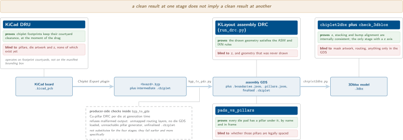
The four checking stages and the artefacts they read. A clean result at one stage does not imply a clean result at another.
Stage |
Runs on |
Proves |
Blind to |
|---|---|---|---|
KiCad DRU |
The board, while you lay out |
Chiplet footprints keep their courtyard clearance |
Everything not yet generated: pillars, die artwork, z |
|
The 3Dblox model derived from the |
z, stacking and bump alignment are internally consistent |
Mask artwork, routing, anything only in the GDS |
KLayout assembly DRC |
The assembly GDS plus its manifests |
The drawn geometry satisfies the ASM and IXN rules |
z, and geometry that was never drawn |
|
The |
Every die pad has a pillar under it |
Whether those pillars are legally spaced |
Stage 1: KiCad design-time rules
Runs on the KiCad board, continuously, while you place and move chiplet footprints.
The ADK generates a DRU section from the same rule registry the KLayout deck
reads, and you paste it into the project’s .kicad_dru:
python kicad/dru/generate_assembly_dru.py \
    --interposer-adapter intm4tm2 \
    --out assembly.kicad_dru
What it proves. That no two chiplet footprints are closer than the assembly
spacing rule, enforced as a courtyard_clearance constraint, plus overlap,
which KiCad’s native courtyard collision check already covers. It proves this
at the moment of the drag, with no export and no external tool run.
What it cannot prove. It is a partial mirror of the deck, by design and by
declaration. Of the 4 assembly rules, only ASM.b has a clean
KiCad expression; ASM.a is delegated to KiCad’s own courtyard collision;
ASM.e and ASM.f have no DRU equivalent and are post-layout only. The
entire interconnect axis is post-layout: at design time the attachment pads do
not exist yet, because hyp_to_gds generates them from the pin lists later.
What it catches that the others miss. The KiCad rule operates on footprint courtyards; the KLayout rule operates on the die bounding box recorded in the boundary manifest. Those are different polygons. A footprint whose courtyard is drawn larger than the die outline, to reserve room for a heat spreader or a handling clearance, is enforced only here: the manifest records the placed die’s bounding box and knows nothing about the reservation you drew around it.
See KiCad DRU generation.
Stage 2: the 3Dblox export and check_3dblox
Runs on a geometric model derived from the finalised .chiplet, not on
any layout file.
python openroad/chiplet2dbx.py \
    --chiplet two_die_interposer.chiplet \
    --out-dir build/3dblox \
    --pins U1=chiplets/metal_test_chiplet.pins.json \
    --pins U2=chiplets/metal_test_chiplet.pins.json
Then, in OpenROAD, read_3dbx build/3dblox/<name>.3dbx loads the assembly and
runs the check_3dblox linter.
This stage has two halves and both matter.
The exporter itself is a checker. It refuses to emit an assembly it cannot
represent faithfully rather than rounding or guessing: a die whose
position.z does not equal the mount surface plus its connection stack
height, to within 1e-6 um; a rotation that is not a multiple of 90 degrees; a
non-canonical orientation token; a die anchored bbox_center, or with no
declared anchor; an unresolvable connection stack; a pin that falls outside the
die’s declared outline; more or fewer than one interposer component.
check_3dblox then lints the loaded database. The open implementation in
OpenROAD runs seven checks: floating components, 3D overlap, connection-region
validity, bump alignment, internal-extension usage, logical connectivity against
a declared netlist, and alignment markers. Supplying per-die --pins lists is
what activates the bump-alignment check, because that is what gives each die a
.bmap.
What it proves. That the assembly is consistent in the third dimension: die heights agree with their attachment stacks, nothing floats, and no two bodies occupy the same volume. This is the only stage with a z axis.
What it cannot prove. Anything about mask artwork. The export is lossy by declaration: artwork, metallurgy, DRC parameters, I/O pads and the boundary manifest have no 3Dblox target and are dropped. A shorted trace, a missing via, a pillar that was never drawn into the GDS: none of it exists in the model being linted.
What it catches that the others miss. Change one die’s position.z by a
micrometre. The KLayout deck cannot see it, because the boundary manifest
records placement polygons with no z at all and layers_def.drc collects them
into a single flat region. The KiCad rules cannot see it either. Here, the
export refuses outright, and a z edited directly into the generated .3dbx
is reported by the linter as an invalid connection.
Stage 3: the KLayout assembly DRC
Runs on the assembly GDS, with the chiplet boundaries injected from the
<gds-stem>.boundaries.json sidecar next to it.
python klayout/drc/run_drc.py \
    --path outputs/layout/two_die_interposer_complete.gds \
    --interposer-adapter intm4tm2 \
    --interconnect-adapter ihp_cupillar \
    --interconnect-methods outputs/layout/two_die_interposer_complete.ixn_methods.json \
    --run_dir /tmp/adk_drc
This is the full rule set: the 4 placement rules on one axis and the 7 interconnect rule forms on the other. The placement axis is always on and selected by the interposer adapter. The interconnect axis is optional and appended only when an interconnect adapter or a per-method file is supplied.
What it proves. That the geometry actually present in the assembly layout satisfies the assembly rules: chiplet boundaries do not overlap and keep their spacing, no degenerate boundary polygon slipped through, attachment geometry that overlaps a chiplet lies fully inside it, and the attachment pads meet the pitch and spacing of the method that owns them. With a per-method file the numbers are scoped per die group instead of assembly-wide, so a fine-pitch vendor method is not checked against a coarse Cu-pillar pitch.
What it cannot prove. Four things, all structural:
Connectivity. The deck compares polygons against rules, never nets against a netlist. An assembly whose dies are placed and attached legally but wired to the wrong nets is clean here. Reconciling the placed assembly against the system netlist is the connectivity axis of assembly-level verification, and it is not part of this preview release.
z. The deck sees a flat 2D region.
ASM.atherefore flags any XY overlap between chiplet boundaries, including dies that a multi-tier assembly would legally stack at different heights. Nothing in the current toolchain produces multi-tier assemblies, so this is not a practical constraint today, but it is baked into the manifest data model and not just into the rule.Absent geometry. The deck checks the pads that exist. If the pillar generation step never ran, there are no pads to violate anything and the deck is clean. This is exactly why
hyp_to_gdsrefuses to emit a GDS when pillars were requested and the pillar generator was unreachable; see Generating the assembly GDS.Fabrication rules that belong to a PDK. The assembly deck does not check the interposer’s own metal, via and pad rules, nor anything internal to a die. Those are the interposer PDK’s and the die PDKs’ decks, and running the assembly DRC is not a substitute for running them.
What it catches that the others miss. Cross-method spacing. When U1 is
attached with cupillar_opt1 and U2 with vendorx_microbump, the deck
emits IXN.x.cupillar_opt1.vendorx_microbump at the larger of the two
declared spacings and checks the pads of one method against the pads of the
other. No design-time rule knows those pads exist, and the 3Dblox model has no
notion of a spacing rule between two dies’ bump fields.
See Running the assembly DRC, Assembly placement rules (ASM) and Interconnect rules (IXN).
Stage 4: the pad-to-pillar alignment check
Runs on the finalised .chiplet, the assembly’s pillar manifest, and a
pad source per die.
python checks/pads_vs_pillars.py \
    --chiplet outputs/two_die_interposer.chiplet \
    --pillars outputs/layout/two_die_interposer_complete.pillars.json \
    --pins U1=chiplets/metal_test_chiplet.pins.json \
    --gds-pads U2 \
    --tolerance-um 1.0 \
    --json report.json
For each die it transforms the die-local pad centres through the die’s placement
(position, rotation, and the flip-chip mirror applied before rotation) into the
canonical assembly frame, and matches them against the as-drawn pillar centres
recorded by the producer. Matching is by pin name where both sides are named,
falling back to greedy nearest-unique matching. Findings are MISALIGNED,
PAD_WITHOUT_PILLAR, PILLAR_WITHOUT_PAD, AMBIGUOUS_MATCH, and with
--strict, NO_PAD_SOURCE.
A named pair beyond tolerance whose pillar is flagged moved_by_auto_resolve
and carries the shift magnitude demotes to a warning within that shift plus
the tolerance: the producer’s collision auto-resolve moved that bump away from
its pad deliberately, so the deviation is expected and must not fail the check.
A bare flag with no magnitude cannot bound the excuse and does not demote.
What it proves. That the correspondence between die pads and interposer pillars holds pad by pad and name by name, in the same frame both sides declare.
What it cannot prove. Nothing about the legality of the pillar field. It
never asks whether two pillars are too close, whether a pillar is inside its
die’s boundary, or whether the geometry drawn in the GDS matches the manifest.
It is a manifest-level check by construction: it compares two declarations, and
the GDS remains the fabrication ground truth. It also needs a pad source per
die, and silently has nothing to say about a die you did not give it one for
unless you pass --strict.
What it catches that the others miss. A uniform offset or a wrong rotation
of an entire pillar field. Shift every pillar of a die by 20 um, or apply the
die’s rotation to the placement but not to its pin list, and the pillar field is
still perfectly spaced: IXN.b and IXN.e pass, ASM.f still finds the
pads inside the die boundary, z is untouched so check_3dblox passes, and the
assembly does not connect. Only this check compares pads against pillars.
Producer-side checks
Two more checks happen inside hyp_to_gds while the geometry is being
generated, before any of the four stages above run. They are not substitutes for
them, but they fail earlier and with a more specific message.
The Cu-pillar DRC runs per die at generation time, using the interposer PDK’s
own bump rules (pad diameter, spacing, enclosure, pitch and pad shape) with the
parameters of that die’s method. Violations are reported and the run continues,
with the complete report written to <stem>_cupillar_drc.json. Pad-to-edge-seal
spacing is not checked here, because the bump list carries no edge-seal geometry;
that rule is enforced by the interposer PDK’s own deck. In the
reference design that report records zero errors and zero warnings across ten
checks over two dies.
The converter also refuses several classes of malformed output outright: more
than half the routing on layers the PDK layer table does not map, a
--with-chiplets run in which no die GDS loaded, a pillar request with no
reachable pillar generator, and a .chiplet that could not be finalised.
Where each stage sits in the flow
The rows below are in the order the stages normally run, which is not the order they are described above:
Stage |
When to run it |
|---|---|
KiCad DRU |
Continuously, from the moment the chiplet footprints are placed. |
KLayout assembly DRC |
After every |
|
After the same run, once the pillar manifest exists. Cheap, no KLayout
session needed unless you use |
|
Whenever die z, thickness, orientation or connection stacks change. The export half fails fast and needs no OpenROAD installation; the linter half needs an OpenROAD image with the 3Dblox commands. |
Note
The KLayout assembly DRC and pads_vs_pillars read artefacts the
producer wrote in the same run, so they are only as current as the last
hyp_to_gds invocation. Re-export before trusting them after a board
edit.
What none of these stages cover
Warning
The ADK is a preview release. These four stages are the geometric axis of
assembly-level verification: they check assembly placement, attachment
geometry, pad correspondence and 3D consistency. They do not reconcile the
assembled layout against the system netlist, which is the connectivity axis
of assembly-level verification and is in the kit’s scope but not part of
this preview release. They also do not check the interposer’s own
fabrication rules, anything internal to a die, or any thermal,
power-integrity or timing property of the assembly. The thermal/,
power/ and timing/ directories of the ADK are reserved names with
README stubs and no implementation. See Roadmap.