
The gap it closes
Why heterogeneous integration
Scaling a single monolithic die has become a poor answer to a growing number of design problems. Reticle limits cap the die area. Yield falls with area, so a large die is expensive twice over. And a monolithic process forces one technology on every function, even where a different node, or a different process family entirely, would suit better.
Heterogeneous integration answers this by disaggregating the system into smaller dies, the chiplets, each built on the technology that suits it, and reassembling them on a carrier. In a 2.5D assembly that carrier is an interposer: a substrate whose only job is to carry dense wiring between the dies mounted on it and out to the package.
That splits the design problem in two. Each chiplet is a conventional die design against a conventional PDK. The assembly is a new problem, and it is the one that had no open tooling.
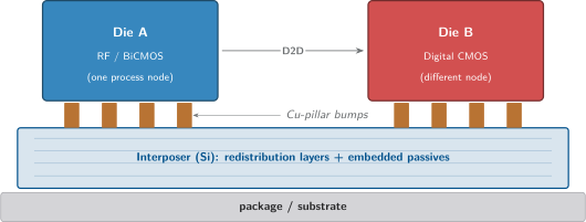
A 2.5D assembly. Two dies built on different process nodes are mounted by Cu-pillar bumps on a silicon interposer that carries the redistribution layers between them.
What was missing
The published open-source flows cover die design thoroughly. Between the finished dies and a fabricable assembly there was very little.
No interposer PDK usable by an open flow. A full process PDK carries several hundred layers, nearly all of them frontend layers an interposer never uses. The interposer needs the upper metal stack, the vias between those metals, and the attachment structures, presented as a technology an open layout tool can load.
No path from die GDS into a board-level design tool. An interposer is laid out much like a very small, very dense PCB, but a PCB tool cannot read GDSII, and a die’s pads are not footprints.
No board tool that works at these scales. PCB tools are built around millimetres. An interposer is designed in micrometres with features and grids down to the nanometre, which stresses assumptions about coordinate precision, rendering and zone filling that hold comfortably at PCB scale.
No way back from board-level routing to fabricable geometry. Routing authored in a board tool has to become mask-level geometry with real via structures from the process, not approximations.
No assembly-level verification of the implemented mask database. This is the central gap. Open assembly linting does exist at the declared-model level, in OpenROAD’s 3Dblox checks, and this page returns to it below. But a DRC deck checks whether shapes are manufacturable on a process, and an LVS deck compares one die’s device netlist against one die’s layout. Neither says anything about the assembly as drawn: whether two dies overlap, whether they respect a placement clearance, whether the attachment structures under a die are consistent with the bumping method the design declared, or whether the assembled result is wired the way the system netlist says it is. Those constraints are not owned by any single PDK, because they are about the relationship between a die and the substrate it sits on. Assembly-level verification is a layer of its own, above the per-die signoff each PDK already provides, and it has two axes: a geometric axis and a connectivity axis. This preview release closes the geometric axis. Reconciling the connectivity of the assembled result against the system netlist is in scope for the ADK and is not part of this preview release.
No interchange format for a placed assembly. Each tool in a chain like this needs to agree on where every die sits, how it is mounted in z, how it is oriented, and which artwork it refers to.
No open 3D view of the result that renders true-to-fabrication geometry derived from the actual GDS, rather than a schematic illustration.
Underneath all of these sits one structural problem. Interposer design lands exactly between two mature tool cultures that disagree about almost everything operational.
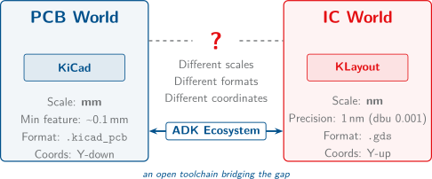
Board-level and IC-level tools differ in scale, file format and coordinate convention. An interposer needs both worlds at once.
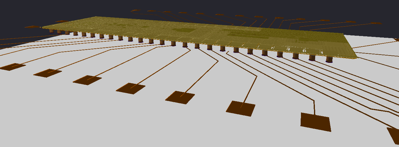
Lateral view of a single die mounted on its Cu pillars above an interposer, with the wire-bond I/O pads and the traces fanning out to them at the interposer edge, rendered from the assembly artefacts this flow produces.
How the ADK closes it
The ADK proper closes the geometric axis of assembly-level verification, and the surrounding ecosystem closes the rest of the chain.
Gap |
What closes it |
|---|---|
Interposer technology for an open flow |
An interposer PDK derived from the backend of the base process. Interposer PDK (OpenIntM4TM2) |
Attachment method decoupled from the substrate |
An interconnect PDK holding the method registry. Interconnect PDK |
Die GDS into a board tool |
A GDS to KiCad converter for footprints, symbols and pin lists. gds2kicad |
Board tool at semiconductor scale |
A KiCad fork hardened for nanometre-scale work. KiCad ADK fork |
Assembly interchange |
The |
Board routing to fabricable geometry |
A HyperLynx to GDS converter using real process via structures. Generating the assembly GDS |
Assembly-level verification, geometric axis |
The ADK rule decks and adapter model. Architecture |
Inspecting the result in 3D |
A viewer rendering GDS-derived geometry. Chiplet Studio |
The approach
Three decisions shape everything else.
Extend mature tools rather than write new ones. The flow is built on KiCad and KLayout, both of which already solve hard problems well. The work is in the gaps between them, not in replacing them.
Keep the assembly rules independent of any substrate. The rules speak in abstract inputs, and a small adapter file maps those to one PDK’s layers. Adding an interposer means adding one file, not editing the rules. See Adapter contract.
Publish the interchange format as a specification, not as an implementation
detail. The .chiplet format is specified, versioned and Apache-2.0, with
reference readers, so a tool outside this ecosystem can participate without
reverse engineering anything.
Positioning
To our knowledge, this is the first open assembly design kit tied to a real, manufacturable open foundry process. The claim is deliberately narrow.
Other open work is active in this space and is complementary rather than competing. While other teams, such as the US-based OpenROAD project, are rapidly advancing open tools in this space, the IHP Open ADK offers complementary capabilities. The 3Dblox assembly format, on the standards track as IEEE P3537, has a BSD-3 licensed implementation in OpenROAD, and the ADK exports to it rather than competing with it. See 3Dblox interoperability.
Note
The interposer process has been fabricated several times at IHP. That is a statement about process maturity. No complete assembly built with this flow has been fabricated and characterised, and this documentation never claims otherwise.