
What the ADK is
An Assembly Design Kit is to a package what a Process Design Kit is to a die. A PDK tells you whether a shape can be manufactured on a given process. An ADK tells you whether a die may sit at a given place, at a given spacing from its neighbours, attached by a given method, and whether the assembly that results is wired the way the system netlist says it is. Those are different questions, they have different owners, and the IHP Open ADK exists because the second set had no open answer.
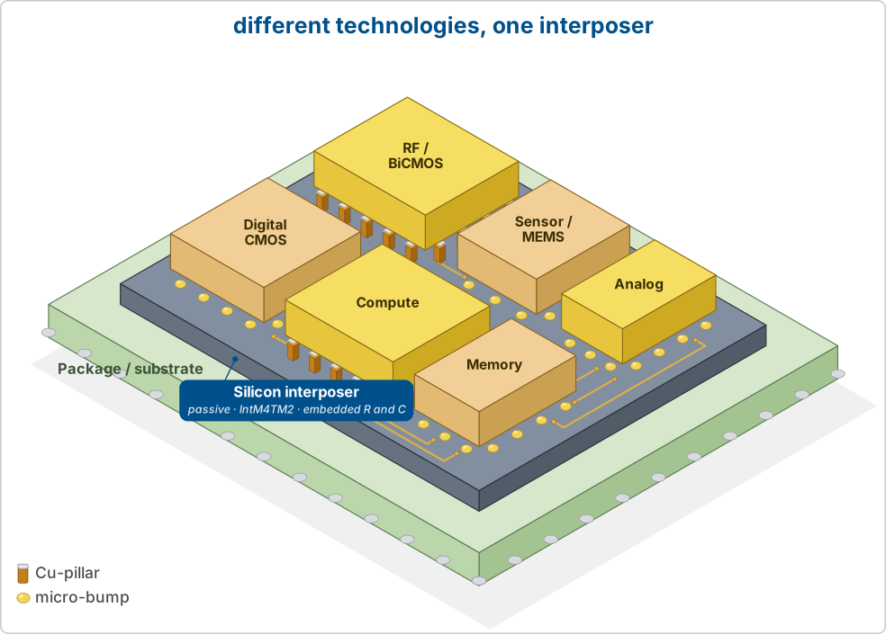
Dies from different process families on one interposer. Each die comes from its own PDK, and the interposer is the attachment surface they share.
The role model
The ADK sits one abstraction layer above all PDKs.
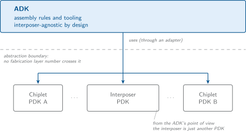
The role model. The ADK sits one abstraction layer above every PDK and reaches each one only through an adapter.
Each PDK owns its own fabrication rules for metal, vias and pads. The ADK governs only the interactions between chiplets and the interposer, never the internal manufacturing of any single PDK. The consequence that matters most is the middle box: from the ADK’s point of view the interposer is just another PDK, so nothing in the assembly rule set is specific to IHP’s IntM4TM2 interposer, or to any interposer.
The abstraction boundary
Rules reference abstract input names only. The mapping from an abstract name
to a PDK-specific fabrication layer lives in a small adapter file, and nowhere
else. The central one is chiplet_attachment_input, the region an interposer
offers for chiplet attachment: on IntM4TM2 the adapter derives it from Cu
pillars, on another substrate it might be solder-bump openings or a
hybrid-bonding pad array, and the rule never asks which. That is what lets one
rule deck check assemblies built on substrates the deck has never heard of.
Architecture lists the abstract inputs and gives the reasoning; Adapter contract specifies what an adapter must declare.
Where assembly verification sits
Assembly verification is a layer of signoff in its own right, above the signoff each die and the interposer already run inside their own PDKs. Like signoff at any other level, it asks two independent questions, and the ADK owns both.
Assembly DRC asks whether the assembly is physically legal: may this die sit here, at this clearance, attached at this density, by this method. It runs on the assembly GDS and its sidecar manifests, and it is what this preview release ships.
Assembly LVS asks whether the assembly is electrically what was intended: are the dies connected to each other the way the system netlist says. It is in the kit’s scope, and no implementation of it is part of this preview release.
Neither question subsumes the other. Legal geometry can implement the wrong netlist, and correct connectivity can be drawn illegally. An assembly is signed off only when both answers are yes.
The geometric axis: assembly DRC
This is the shipped axis, and it is the subject of most of this site. It holds
two families of rule, each driven by its own adapter and both reading the
assembly through abstract inputs rather than through a fabrication layer number.
ASM.* answers where a die may sit, clearance and collision between chiplet
outlines, and is always on; IXN.* answers how dense, by what method, the
bump-to-bump pitch and spacing that belong to the bumping method rather than to
the substrate, and is optional. Swapping the interposer adapter changes the
substrate, swapping the interconnect adapter changes the bumping method, and
neither touches the rules. See Assembly placement rules (ASM) and
Interconnect rules (IXN).
Geometric checking in a 2.5D assembly also splits into three levels, and the first two are ordinary PDK DRC. Each die is checked against its own PDK’s rule deck, and the interposer is checked against the interposer PDK’s. Neither of those checks changes because the part ends up in an assembly, and neither can be extended to cover the assembly: a rule deck runs on one layout, in one technology, and no PDK deck sees two dies at once. The space between the dies, and the attachment geometry that lands them on the interposer, belongs to a third level that no PDK owns. That level is what the ADK ships.
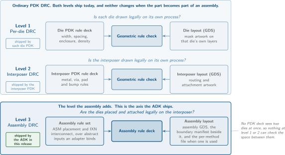
The three levels at which an assembly’s geometry is checked against a rule set. Levels 1 and 2 are ordinary PDK DRC. Level 3, assembly DRC, is the level the assembly adds, and it is what this preview release ships.
It is four complementary checks, each blind to something the others see: a design-time pass inside KiCad, a database-level lint of the exported 3Dblox model, the KLayout rule deck on the finished GDS, and a pad-to-pillar alignment check. Verification stages sets out what each one proves and, more usefully, what it does not.
What the geometric axis cannot tell you is whether the nets are right. It sees polygons, clearances and areas. Two dies can be perfectly placed and perfectly bumped, and still be wired to the wrong nets.
The connectivity axis: assembly LVS
Layout versus schematic verification is mature inside a single die. A 2.5D assembly splits the same question into three levels, and only the first two have open tooling today.
Per-die LVS compares each die against its own schematic netlist, with devices extracted from the die layout by the die’s own PDK. Every PDK already ships this, and it runs unchanged when the die becomes part of an assembly.
Interposer LVS compares the interposer against its own netlist. From the ADK’s point of view the interposer is just another PDK part, so this is ordinary PDK LVS with nothing assembly-specific about it, and the interposer PDK ships the deck. Interposer PDK (OpenIntM4TM2) documents the deck for IntM4TM2.
Assembly LVS asks whether the dies are connected to each other as the system intends. The reference is a system netlist that names die pins and the nets that join them. The implementation is the placed set of layouts, where a connection is realised by a pad landing on the interconnect under it, plus the interposer routing between those landings. This is the level at which chiplet assemblies fail in practice: a mirrored die, a swapped pad, a placement shifted far enough that a bump misses its pad.
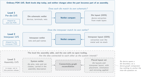
The three levels at which an assembly’s connectivity is compared against a reference, laid out to be read against the geometric axis above. Levels 1 and 2 are ordinary PDK LVS. Level 3, assembly LVS, is within the ADK’s scope and no implementation of it is part of this preview release.
Device-graph comparators do not reach the third level. A classical netlist comparator establishes correspondence by matching devices and their terminals, then checks the nets between them. But the devices in a 2.5D assembly sit inside the dies, already matched by each die’s own PDK, and the few passives the interposer carries correspond to nothing in the system netlist. No device participates in the inter-die connectivity, so nothing spanning a die boundary is left to anchor the correspondence on. The abstraction is wrong for the problem rather than misconfigured. The question is instead a reconciliation between connectivity graphs, in which a net is a set of component, pin and layer endpoints.
Roadmap states what would have to exist before this axis ships.
What the ADK is not
It is not a PDK. It ships no device models, no PCells and no fabrication rules.
It is not a place-and-route tool. It checks placements that a designer or another tool produced.
It does not verify inter-die connectivity today. The rule set that ships in this preview is geometric. Assembly-level connectivity verification is the other axis, it is in the kit’s scope, and no implementation of it is part of this preview release.
It is not a substitute for per-die PDK signoff. It is the layer above it, and this preview release ships its geometric axis.
Where the boundary comes from
Chiplet boundaries are not read from a fabrication layer. They travel in a per-assembly sidecar, <gds-stem>.boundaries.json,
which the producer emits next to the assembly GDS and the DRC runner discovers
automatically.
An earlier revision did stamp boundaries onto a GDS layer, exchange0 at
190/0. That number is a real IHP SG13G2 layer, so pinning a cross-PDK assembly
contract to it was an abstraction leak, and it risked colliding with a chiplet’s
own geometry on that layer. The manifest is PDK-agnostic by construction and
cannot alias anything. The old path survives only behind
--legacy-exchange0, for checking a pre-migration GDS.
Boundary manifest is the normative description.
A note on maturity
Warning
The ADK is a Preview Release. The interposer process has been fabricated several times at IHP, which is a statement about process maturity rather than about a complete assembly. The assembly rule values shipped in the registries are engineering defaults, not foundry-sanctioned assembly rules. Read Registries and schemas before treating any number here as a specification.