
KiCad ADK fork
The layout tool of this flow is a fork of KiCad, IHP-GmbH/KiCad-ADK-MOD. It is the tool in
which you place dies, draw the interposer, route it, and from which the assembly
leaves as a .chiplet file and a HyperLynx netlist.
Why a fork
Pcbnew already counts every coordinate in integer nanometres, so a 10 nm feature is representable without any change. What is not representable is the set of assumptions built on top of that number.
Upstream KiCad is a PCB tool, and a PCB is a millimetre-scale object. Constants, validation limits, default grids, drawing decorations and intermediate arithmetic were all chosen for designs whose smallest feature is roughly 0.1 mm. An interposer built on the IntM4TM2 technology has features three to four orders of magnitude smaller. Every one of those PCB-scale assumptions then shows up as a concrete failure:
Dialogs refuse a track width of 10 nm because a hardcoded minimum rejects it.
The nearest grid a user can snap to is 10 um, which is coarser than the feature being drawn.
A locked-item shadow sized from the silkscreen line width (about 0.15 mm) drawn around a 10 nm via is 15000 times larger than the via.
A squared distance accumulated in 32-bit arithmetic overflows once the two points are more than about 46 um apart, after which a “nearest item” search compares wrapped negative values and picks the wrong item.
The zone filler prunes with a fixed 1 um epsilon, which is larger than the geometry it is pruning.
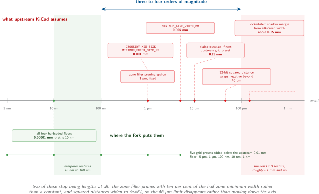
The same failures on a logarithmic length axis. Every upstream constant was chosen for the band on the right; the geometry being drawn sits in the band on the left. The fork moves each constant down, or replaces it with a value proportional to the design.
Most of this is not a bug in KiCad so much as a tool being used three to four orders of magnitude outside the range it was designed for. The 32-bit squared distance is the exception: a plain upstream overflow that nothing about interposer work causes, fixed here because a flow that depends on picking the right footprint under the cursor cannot live with it.
The fork is therefore the set of changes that make those assumptions scale with the design rather than with the historical PCB default, plus the two export formats the assembly flow needs and upstream has no reason to carry.
Note
The fork is a fork, not a patch queue rebased onto every upstream release. It branched from the KiCad development line in late 2025, at a commit on the 9.99 development version (the line that becomes KiCad 10). Nothing here is upstreamed, and no upstream compatibility promise is made beyond what the file formats already guarantee.
The delta versus upstream
The fork diverges from its upstream base at commit cc80f778ec (28 October
2025) and carries 42 commits at the revision this documentation is built
against. Those commits touch 35 files under the KiCad source tree, of which four
are new: the chiplet exporter (pcbnew/exporters/export_chiplet.cpp and its
header), a public header for the HyperLynx exporter, and a SWIG interface file.
The rest are edits to existing files. Five further files at the repository root
are packaging rather than source: a build Dockerfile, an AppImage script, a
launch script, the change log and an ignore-list edit.
That is a deliberately small delta. It is small because almost every change is of the form “replace a constant with something proportional to the design”, not “add a subsystem”. Outside the chiplet exporter, the largest single edit is the HyperLynx writer at about 90 changed lines; most of the rest are a handful of lines each.
The fork carries its own change log in NANOMETER_MODIFICATIONS.md at the
repository root, which is the authoritative per-symbol record.
Geometry limits
Four hardcoded floors, in three files, are lowered to 0.00001 mm, which is
10 nm. Their upstream values are not uniform: 0.001 mm for GEOMETRY_MIN_SIZE
and MINIMUM_ERROR_SIZE_MM, 0.005 mm for MINIMUM_LINE_WIDTH_MM and
0.01 mm for the dialog’s minSize. All four are PCB-scale limits, and all
four reject interposer geometry:
File |
Symbol |
Effect |
|---|---|---|
|
|
The router and DRC accept track widths and via diameters down to 10 nm. |
|
|
Board Setup constraints accept values down to 10 nm without a validation error. |
|
file-scope |
The Track and Via Properties dialog clamps to 10 nm instead of 0.01 mm. |
10 nm is a practical floor, not a physical one: KiCad’s internal unit is 1 nm, so 10 nm leaves an order of magnitude of headroom for rounding in intermediate geometry.
Units and grids
EDA_UNITS::UM already exists upstream. What the fork adds is the ability to
select it and the precision to make it useful.
common/tool/actions.cppandinclude/tool/actions.hdeclare a newACTIONS::micrometersUnitsaction (common.Control.micrometerUnits, friendly name “Micrometers”), wired into unit switching incommon/tool/common_tools.cppand into unit cycling incommon/eda_draw_frame.cpp.The action is added to the left toolbar of the PCB editor, the footprint editor and the footprint viewer, alongside mm, inch and mils.
common/eda_units.cppformats micrometre message text with%.4finstead of%.1f, so 1 nm reads as0.0010 umrather than0.0 um. Full-precision edit fields are unaffected: micrometres fall through to the%.10fdefault path there, so nothing is truncated on input.common/settings/app_settings.cppadds five grid presets below the upstream 0.01 mm floor: 5 um, 1 um, 100 nm, 10 nm and 1 nm. 1 nm is the hard floor because that is the internal unit.The same file makes micrometres the default unit for the PCB tools (
system.unitsandsystem.last_metric_units). Eeschema and the symbol editor keep mils. A fresh container therefore opens pcbnew already in the units the flow works in.
Rendering at extreme zoom
Two independent rendering problems appear once the viewport is scaled to micrometre features.
The first is decoration sizing, in pcbnew/pcb_painter.cpp. The locked-item
shadow margin defaults to four times the silkscreen line thickness, and the hole
wall thickness to the plating thickness times an advanced-config multiplier.
Both are absolute lengths. Against nanometre geometry they swamp the object they
decorate. The fork clamps each to a fraction of the item it is drawn on: the via
shadow to a quarter of the via width, the hole wall to a quarter of the drill
size, the track shadow to the track width. At PCB scale the clamps never
trigger, so standard boards look exactly as before.
The second is coordinate range, in common/gal/cairo/cairo_gal.cpp. At
extreme zoom, transforming an off-screen world coordinate to screen space
produces a pixel coordinate far outside any plausible display. When pixman
computes region extents from it the value exceeds the 32-bit range and the
render aborts with repeated pixman_region32_init_rect: Invalid rectangle
passed messages. CAIRO_GAL_BASE::xform() now clamps its output to plus or
minus 1e8 pixels, which is far outside the visible canvas and therefore
invisible in effect. common/gal/cairo/cairo_compositor.cpp and CAIRO_GAL::allocateBitmaps()
additionally floor surface dimensions at one pixel, so a zero-sized surface can
never be allocated.
Integer arithmetic
Squared distances are the failure mode. With a 1 nm internal unit, two points 46.3 um apart already produce a squared distance at the 32-bit signed limit. Beyond that the value wraps negative, and any “nearest” search silently picks the wrong answer.
Three sites are widened:
Site |
Change |
|---|---|
|
|
|
|
|
The differential-pair gap is computed with |
Zone filling
pcbnew/zone_filler.cpp used a fixed pruning epsilon of 1 um. Because the
epsilon is subtracted from half the zone minimum width, any zone with a minimum
width below roughly 4 um had its pruning step effectively skipped. The fork
replaces the constant with std::max( half_min_width / 10, 1 ), that is 10
per cent of the half minimum width with a floor of one internal unit. The hatch
fill margin gets the same treatment against GetMinThickness().
Note
This one changes behaviour at PCB scale too. A board with a 0.25 mm zone minimum width now prunes with a 12.5 um epsilon rather than 1 um. The fills are more conservative than upstream’s, not less, but they are not identical. If you use this fork for ordinary PCB work, expect zone fill differences.
Export precision, HyperLynx
The HyperLynx writer in pcbnew/exporters/export_hyperlynx.cpp changes in
three ways, all of them required by hyp_to_gds.py downstream.
Metric output. The header is {UNITS=METRIC LENGTH} instead of
{UNITS=ENGLISH LENGTH}, and the conversion helper iu2hyp returns
iu / ( PCB_IU_PER_MM * 1000.0 ), that is metres, instead of dividing by
0.0254 to reach inches. The inch factor is not exactly representable in binary
floating point, so the imperial path lost precision on every coordinate. At PCB
scale that loss is far below the manufacturing tolerance; at interposer scale it
is a substantial fraction of a feature. A 200 um trace now exports as
W=0.0002000000.
Explicit via layer stacks. writeSinglePadStack no longer collapses a
padstack that spans the whole layer mask into the MDEF master-definition
form. Every via is written as an explicit per-layer list. MDEF is a size
optimisation that assumes the reader knows the stackup; hyp_to_gds.py needs
to map each padstack level onto a named PDK layer, and cannot do that from a
mask.
Device records carry placement and a GDS link. Upstream writes only
(? REF="U1" L="Top"): a device belongs to a layer and nothing more, because
a HyperLynx consumer is expected to get geometry from the pads. writeDevices
now adds the footprint position and rotation, and a footprint field named
GDS_FILE when it is not empty:
(? REF="U1" L="Top" X=... Y=... R=... GDS_FILE="/path/to/cell.gds")
Y is negated so device positions share the sign convention the wire coordinates
already use. The GDS_FILE link is how a placed footprint keeps a reference
to the artwork it stands for, so that the converter can instantiate the real die
layout rather than a rectangle. gds2kicad writes that field when it generates
the footprint, so the link is usually established without anyone typing a path.
See gds2kicad.
All three quoted tokens pass through sanitizeHypToken() first, which maps an
embedded double quote to an apostrophe and a newline, carriage return or tab to
a space. A reference, a renamed layer or a user-typed path is third-party data,
and one quote in it would close the field early and cost the consumer the whole
device record. The plugin’s Python writer carries the same function, because the
two outputs are compared byte for byte.
Export precision, chiplet
pcbnew/exporters/export_chiplet.cpp is new, about 650 lines, and has no
upstream counterpart. CHIPLET_EXPORTER::WriteYAML emits the .chiplet
assembly description:
Reads
INTERPOSER_LYPfrom the board properties, falling back to the project text variables, to name the interposer technology. OptionalINTERPOSER_ADAPTERandINTERCONNECT_ADAPTERtext variables select the ADK rule adapters, defaulting tointm4tm2and to nothing respectively.Walks the footprints, separating interposer I/O pads (those carrying an
IO_CLASSfield, nested under the interposer component’sio_pads) from chiplet dies, and reads each die’sGDS_FILE,LYP_FILEandORIENTATIONfields. A die markedORIENTATION = "flip_chip"is emitted withconnection: cupillar_opt2,orientation: flip_chipandz: 0.0, deferring vertical placement to the consumer that understands flip-chip stacking; a face-up die onF_Cugets no orientation key and takes its z from the board thickness. Diethicknessis written as a0.0placeholder here and filled in downstream.Takes each component’s width and height from its courtyard (
F_CrtYdorB_CrtYd) when one exists, falling back to the footprint bounding box.Converts KiCad’s Y-down global frame to a Y-up Cartesian frame anchored on the
Edge.Cutsbounding box, sox = pos.x - bbox.leftandy = bbox.bottom - pos.y, then scales to micrometres.Writes a fixed
connection_stackslibrary of four bonding stacks (cupillar_opt1,cupillar_opt2,cupillar_opt3andsbump_sac305), each with its layer materials, heights and diameters, so a consumer has geometry for the common cases without a hand-written definition. The values and the descriptions in the emitted YAML name the bumping vendor’s Cu-pillar table they come from.
Coordinates are written with six decimal places in micrometres, which is 1 pm of resolution. Four decimals, the earlier setting, quantises at 100 pm, which is visible at these scales. Rotations keep four decimal degrees.
Note
The file the C++ exporter writes is not the canonical .chiplet. It is
anchored on the PCB bounding box, and it says so: it carries a _metadata
block with frame: pcb-bbox-corner and finalize_required: true. The
canonical frame is anchored on the generated GDS bounding box, and only
hyp_to_gds.py --update-chiplet-file can produce it, because only that
step knows where the GDS bounding box ends up. Readers must refuse a file
with finalize_required: true. Coordinate frames has
the full contract.
Python surface
Both exporters are exposed to Python, because the plugin, not a menu, drives
the flow. pcbnew/python/swig/pcbnew.i includes export_chiplet.h and
export_hyperlynx.h, making these two functions callable from a script:
ExportBoardToChipletFile(board, output_path)    # -> bool
ExportBoardToHyperlynxFile(board, output_path)  # -> bool
pcbnew/python/swig/board_stackup.i is a new interface file that exposes
BOARD_STACKUP and BOARD_STACKUP_ITEM, so a Python writer can iterate the
physical stackup returned by BOARD_DESIGN_SETTINGS::GetStackupDescriptor().
The plugin’s Python HyperLynx writer needs this to reproduce the C++ exporter’s
output byte for byte.
Stability
One fix in the fork is unrelated to scale. Autosave history savers in
common/eda_base_frame.cpp, eeschema/sch_edit_frame.cpp and
pcbnew/pcb_edit_frame.cpp were keyed by pointers that SetBoard() and
SetSchematic() delete and replace, which is a use-after-free. They are now
keyed by stable addresses.
Where the exports live in the UI
This has moved, and older material describes the old arrangement.
Chiplet export has no native menu action. The C++
CHIPLET_EXPORTERis reachable only throughExportBoardToChipletFile, and the plugin at Tools > External Plugins > Chiplet Export is its sole entry point. See Chiplet export plugin for why.HyperLynx export was removed along with it. The headless entry points remain available through SWIG, so the plugin still drives the same
HYPERLYNX_EXPORTERand stages the.hypinto its output directory on every run. There is no File > Export menu action for it in the fork.
How it is built and pinned
The fork is not a submodule of this documentation repository. It is a submodule
of IHP-GmbH/ADK-Tools at tools/kicad, and that gitlink is the pin: the
documentation you are reading was checked against
5d12a2566750832a5bdd94ebe520f756901762e4.
The container builds it from source in a dedicated stage:
cmake -G Ninja -S /src/kicad -B /build/kicad \
    -DCMAKE_BUILD_TYPE=Release \
    -DCMAKE_INSTALL_PREFIX=/usr \
    -DKICAD_SCRIPTING_WXPYTHON=ON \
    -DKICAD_USE_OCC=ON \
    -DKICAD_SPICE=ON \
    -DKICAD_BUILD_QA_TESTS=OFF
KICAD_SCRIPTING_WXPYTHON=ON is the load-bearing flag. It installs the
pcbnew Python module into the system dist-packages, which is what lets
the export pipeline run headless from any interpreter, not only from inside the
GUI. The container’s regeneration and verification steps depend on it.
Two consequences of the fork’s version follow from this:
The fork reports version 9.99, the development line that becomes KiCad 10, so its configuration lives under
.config/kicad/9.99/.It predates the
.kicad_symdirlibrary format, so the container ships the official KiCad v9 symbol and footprint libraries (pinned by theKICAD_LIBS_TAGbuild argument, 9.0.9.1 at the documented revision) rather than a newer set. All stock symbol libraries are registered; only a small curated footprint table is, because enumerating the roughly 15000 stock footprints on every launch dominates startup time in a container with no persistent cache. The full footprint set stays on disk under/usr/share/kicad/footprintsand can be re-added from Preferences > Manage Footprint Libraries.
The image also forces Mesa’s software renderer for every GUI
(LIBGL_ALWAYS_SOFTWARE=1, GALLIUM_DRIVER=llvmpipe), which KiCad’s
accelerated canvas needs in a container with no GPU device. See
The ADK-Tools image.
An AppImage recipe (create_appimage.sh, plus an APPDIR lookup in
common/paths.cpp so the bundle finds its own resources) also lives in the
fork, for running the tool on a host without Docker.
What this page does not assert
Everything above was read out of the pinned fork checkout. Two things it does not establish:
No claim is made about behaviour on non-Linux hosts. The fork is built and exercised on Ubuntu 24.04 in the container. Nothing in the delta is platform-specific, but nothing has been checked elsewhere either.
No claim is made that the fork tracks upstream. Upstream KiCad has moved on since the fork point. Whether a given upstream fix is present depends entirely on whether it predates
cc80f778ec.