
Chiplet Studio
Chiplet Studio is the interactive viewer of the toolchain. It opens a
.chiplet assembly file, renders the assembly in 3D from the layouts the file
points at, and lets you drill down into any component’s real GDS or OASIS in a
2D KLayout view without leaving the application. It also carries three surfaces
that turn it from a viewer into a workbench: a connectivity graph, an embedded
Python interpreter, and a subprocess pipeline runner driven by the assembly
file’s own flow: block.
Repository: IHP-GmbH/chiplet-studio. Licensed GPL-3.0-or-later, because it links KLayout as a library.
Warning
Chiplet Studio is a Preview Release. Treat what it draws as a design aid. Nothing it displays is a verification verdict: the checks live in the ADK DRC and in the export-time consistency tests, not in the viewer. See Verification stages.
What it is for
The problem it solves is that a 2.5D assembly has no single file you can open. The interposer is one layout, each die is another, the placement lives in the assembly file, and the attachment bodies are not in any of them: they are generated. Reviewing a placement therefore used to mean reading coordinates.
Chiplet Studio resolves all of those inputs and draws the result. The important consequence is that the 3D view is not a schematic-style diagram of boxes. In either of its detailed modes it extrudes the actual polygons read out of each component’s GDS, layer by layer, at the elevations the technology’s stackup declares.
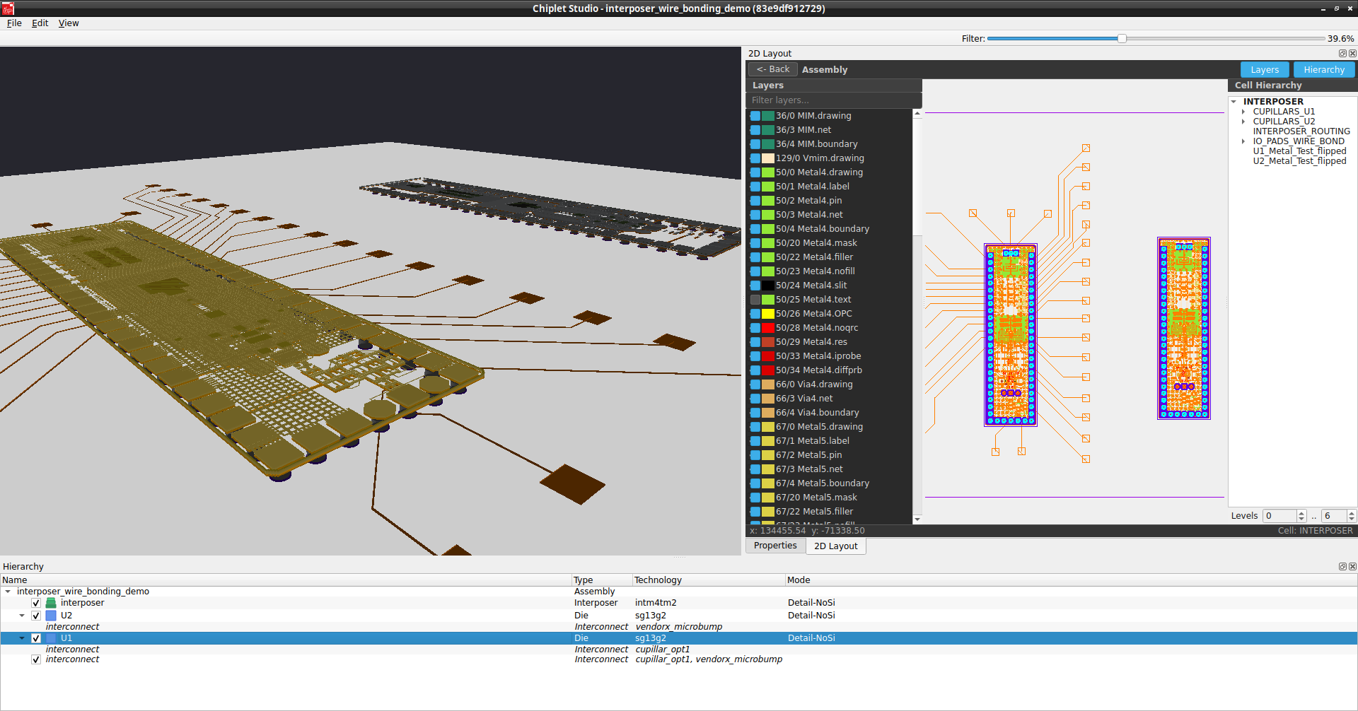
Chiplet Studio on a two-die wire-bonding demo, a simplified variant of the
reference design rather than the shipped example itself. All three components
are in DetailedNoSubstrate mode, abbreviated Detail-NoSi in the Mode
column, so the layouts’ own polygons are extruded with the silicon bulk slab
left out. The centre panel is the 2D view in assembly mode, carrying the
interposer technology’s own layer table. The cell hierarchy is on the right,
and the assembly hierarchy along the bottom gives each component its
technology (intm4tm2, sg13g2) and each die its interconnect method
(cupillar_opt1, vendorx_microbump).
Note
Chiplet Studio is not the only open 3D layout viewer: OpenROAD ships one, and
GDS3D, whose tessellation code Chiplet Studio links, predates both. What is
specific here is that the unit of display is the assembly, resolved through
the .chiplet format and the two PDK axes, rather than a single die.
Opening an assembly
The executable opens the GUI. Pass a .chiplet file to load an assembly on
startup:
chiplet-studio                             # empty session
chiplet-studio path/to/assembly.chiplet
File > Open does the same from the GUI. Loading runs on a worker thread and
is cancellable, so a large assembly does not freeze the window. File > Reload
re-reads the file from disk, which is the fast loop when you are editing the
assembly file in a text editor beside the viewer.
The parse itself is not implemented in Chiplet Studio. src/formats/ is a thin
consumer that delegates .chiplet reading and validation to the vendored
Apache-2.0 chiplet_format_io reference library, a copy of the specification
repository’s reader, and maps the resulting document into the studio’s own
Assembly model. That vendoring is identical to the specification’s reference reader. A file the
specification rejects is rejected here for the same reason and with the same
message, so the viewer cannot quietly accept something the rest of the flow will
not. See The .chiplet assembly file.
Autosave runs on a timer, and a crash-recovery dialog offers the recovered
assembly on the next start. A recovered assembly is deliberately detached from
its path and needs Save As.
Importing a bare GDS
File > Import GDS (Ctrl+I) opens a single layout that has no assembly
file. The importer detects the top cell and the bounding box, then synthesises a
minimal .chiplet around it and loads that through the normal path. This is
deliberate: the imported layout is validated by the same format_version gate
as any other assembly, and the synthesised file is a real artefact you can keep
and edit.
The import dialog asks for the technology. Naming one of the supported ids
(sg13g2, sg13cmos5l, sky130, gf180, intm4tm2) is enough:
the studio resolves that id to a shipped stackup and colour scheme on its own.
Leaving it empty produces a custom_imported technology that carries whatever
layer-properties file and stackup YAML you supply.
The 3D view
Camera control is an orbit camera: drag to rotate, wheel to zoom, and a rubber
band selects. Ctrl+B toggles the base plane and Ctrl+M the scene
mini-map. File > Export PNG (Ctrl+E) renders the current view offscreen
at a chosen resolution, which is how you get a figure out of it.
Render modes
Render mode is per component, not global, so an assembly can show one die in full detail while its neighbours stay as cheap solids.
Each mode has two names. The first column below is the name the C++ enumeration
and the scripting surface use; the second is the abbreviation the hierarchy
panel prints in its Mode column, which is the one you read off a screenshot. The
right-click Render Mode menu spells the two detailed modes out again as
Detailed (with Si bulk) and Detailed (no Si bulk).
Mode |
In the panel |
What it draws |
|---|---|---|
|
|
Nothing. |
|
|
Bounding-box edges only. |
|
|
Semi-transparent solid block at the declared dimensions. |
|
|
Opaque solid block at the declared dimensions. |
|
|
Full per-layer GDS tessellation, including the silicon bulk slab. |
|
|
The same tessellation with the bulk slab omitted. |
The last two are the modes that read the layout. Polygons are extracted through
KLayout’s db library, triangulated by the GDS3D tessellator (with a fallback
to an ear-clipping implementation when GDS3D returns a degenerate result for a
polygon), and extruded between the z_bottom and z_top the stackup gives
for that layer and datatype.
Two conventions from the .chiplet coordinate contract are honoured at mesh
build time rather than at placement time, and both are visible in the render.
A die declared flip_chip has its layer elevations inverted so the topmost
metal sits at the mounting surface, and each component’s anchor field
(gds_origin or bbox_center) decides whether its mesh is built around its
own GDS origin or centred on its bounding box. Dies produced by gds2kicad
use gds_origin; interposers use bbox_center. See
Coordinate frames.
The Filter slider on the View Mode toolbar hides polygons below a percentage of the selected component’s shape-area distribution. On a real die the polygon count is dominated by fill and by tiny features; pushing the filter up leaves the structures that are actually worth looking at and makes the view interactive again.
Black-box chiplets
A chiplet from a closed PDK arrives as a GDS with pads, pad names and an outline and no layer-properties file at all. Rendering that against a real stackup would be wrong, and rendering every unmodelled layer as a full-thickness slab would produce a vertical explosion of meaningless geometry.
The studio detects the case (no .lyp and no resolved stackup) and
augments the stackup with two canonical roles instead: outline becomes the
die body at the declared thickness, and pad becomes a 1 um plane flush on
the die’s active face, moved to the bottom face for a flip-chip die. Colours for
those two roles come from a user-editable file,
configs/stackups/colors/generic/blackbox.yaml, so the black-box look is a
knob rather than a hardcode. The layer numbers involved are the ones the ADK’s
config/chiplet_pads.json registry declares for black-box chiplets, which is
what keeps the producer and the viewer in agreement. See
Registries and schemas.
Layer stackups
A stackup answers one question per GDS layer: where does it start in z, and how thick is it. Chiplet Studio resolves that answer from several sources in order of specificity.
An explicit
stackup:path on the technology in the.chipletfile. This wins, and it is resolved through the same${VAR}and relative-path chain as every other path in the file.A shipped stackup for a supported PDK id.
configs/stackups/carriesihp-sg13g2.yaml,ihp-sg13cmos5l.yaml,intm4tm2.yaml,sky130.yamlandgf180mcu.yaml.A GDS3D techfile sitting beside the technology’s
.lyp, at<dir>/techfile/<stem>.txt, which is auto-loaded when present.A default stacking derived from the
.lypitself, as a last resort.
The YAML dialect is the BlenderGDS one: top-level keys are layer names, each
carrying index (GDS layer), type (datatype), z and height in
micrometres.
Metal4:
  index: 50
  type: 0
  z: 3.66
  height: 0.49
Note
The shipped stackups render the silicon bulk at 50 um and say so in a comment,
although the real SG13G2 wafer is 750 um. A true-scale substrate dwarfs a
14 um back end and a 48 um pillar stack and makes the assembly view unusable.
Restore height: 750.0 in the Substrate entry if you need the physical
proportion, for example when preparing geometry for a thermal or mechanical
study.
Attachment bodies
The Cu pillars and solder balls between a die and the interposer are not in either layout, and they do not belong to the interposer PDK. They come from the interconnect PDK as stackup fragments, one per method id, and are merged into the render at load time.
The join is explicit rather than positional. An interposer stackup declares
attachment_surface_z, the surface it offers to attachment bodies, which is
the exposed pad top rather than the maximum z of the stack (the passivation
around the opening rises above the real mounting surface). Each interconnect
fragment declares z_reference: attachment_surface, so its own z values are
relative and get offset by whatever the interposer declared. That is what lets
the same cupillar_opt2 fragment sit correctly on a different interposer.
Resolution of which fragments to use is one function, resolveInterconnectKeys.
Method ids that resolve to a fragment win, so per-die methods render with their
own option’s heights. The older adapter-keyed fragments (ihp_cupillar,
ihp_sbump) are used only when no method id resolves at all, because they
carry family-default heights that must not overwrite a resolved per-method
value. An id that resolves to no fragment is skipped without complaint, because
a connection: id is not required to be a manifest method id: legacy and
custom connection stacks are legitimate, and the adapter fallback covers them.
What it is loud about is an elevation conflict. The three Cu-pillar options
share layers 500 and 501, so an assembly mixing them gives the merged render two
different heights for one layer and datatype. The studio draws the taller body
and warns which fragment it came from. Seating is unaffected, because each die
is seated from its own resolved fragment rather than from the merged view.
Without the interconnect PDK on disk, the bodies simply do not render. See Interconnect PDK.
The Layer Z spin box on the View Mode toolbar exaggerates the spacing between stackup layers in either detailed mode so you can see into the stack. It is visualisation only and never touches the saved model, and it is enabled only for a single imported die: on a multi-component assembly the exploded fans of neighbouring components would interleave.
The 2D drill-down
F4 toggles the 2D panel. It embeds KLayout’s own layout view widget, so
what you get is KLayout’s rendering, its layer panel and its cell hierarchy, not
a reimplementation.
The panel has two modes. In assembly mode it shows the assembly layout as a
whole. It resolves that layout by looking first at the assembly file’s explicit
assembly_gds field, then by deriving a merged-layout name from the
interposer’s own layout path (*_interposer.gds becomes *_complete.gds,
otherwise *_complete is appended). If no merged layout exists on disk it
falls back to the interposer’s own GDS and labels the view to say so, because in
that state the dies are genuinely not in the picture.
In drill-down mode you are inside one component’s layout. Selecting a
component in the 3D view or in the hierarchy panel drills into it; the header
shows the component name and technology, a combo box selects the cell, and the
status line gives live coordinates. The mapping between GDS cells and assembly
components is kept by a dedicated CellComponentMapper, which is what makes
selection sync work in both directions instead of only from the tree down.
Selection is synchronised across the 3D view, the hierarchy panel, the properties panel and the net graph. The properties panel shows the selected component’s identity, position, dimensions and technology, with unit conversion.
The net graph
Ctrl+G opens the net graph. It draws the assembly’s connectivity as
components (nodes) joined by nets (edges), with a hub node inserted for nets that
have more than two endpoints so a power net does not turn into a mesh of
pairwise edges.
Nets are classified, and the classification drives both colour and filtering:
Signal, Power, Ground, DiffPair, NC and Interface, the
last being an inter-chiplet interface signal. A net can also be flagged
external, meaning it leaves the package boundary, for instance because it
terminates on an interposer IO pad for wire bonding.
Selecting a component highlights its nodes and its incident edges. The edges carry their two endpoint component ids as item data, so highlighting matches by netlist relationship rather than by pixel proximity.
The graph is only as good as the netlist in the assembly file: it reads the
.chiplet netlist and does no extraction of its own. An assembly with no
netlist shows an empty-state panel. The netlist: block is described in
Components and optional blocks.
The flow pipeline
An assembly file can carry a flow: block, and the studio will run it. The
Flow Pipeline dock shows each step with its status, elapsed time, a per-step run
button, and the captured output of whichever step you select.
Note
The dock has no menu entry on purpose. It reveals itself when the loaded
assembly defines a flow: and stays hidden otherwise, so it never presents
an empty panel. The project README.md still lists it under
View > Flow Pipeline; the code is the accurate description.
A step is one subprocess invocation:
flow:
  working_directory: /tmp/flow_test
  environment:
    PDK_ROOT: /opt/pdk
  steps:
    - id: step_hello
      name: "Hello World"
      tool: /bin/echo
      args: ["hello", "${assembly.name}"]
      output_files: [hello.txt]

    - id: step_goodbye
      name: "Goodbye"
      tool: /bin/echo
      args: ["goodbye"]
      depends_on: [step_hello]
      input_files: [hello.txt]
Steps declare depends_on, and the engine topologically sorts them before
running, so Run All executes in dependency order rather than file order.
Arguments support variable substitution against the loaded model:
${assembly.field}, ${component.ID.field} and ${technology.ID.field}
are resolved at parse time, and an unresolved variable is a parse error rather
than an empty string passed to a tool.
The engine itself contains no domain knowledge. It resolves dependencies, starts
processes, captures stdout and stderr, tracks exit codes, and reports status.
Everything that makes a pipeline meaningful lives in the assembly file. The
shipped examples/openroad_3dblox/ demo uses this to run two real steps
against an assembly: exporting it to 3Dblox with the ADK’s chiplet2dbx, then
loading that export with read_3dbx and linting it with check_3dblox in an
OpenROAD container, with the step failing on any linter warning rather than only
on a crash. See OpenROAD 3Dblox export and 3Dblox interoperability.
Python scripting
View > Python Console (Ctrl plus backtick) opens an embedded
interpreter. The
chiplet_studio module, built with pybind11, exposes the same model the GUI
edits, so a script drives the live assembly rather than a copy of it.
import chiplet_studio as cs

asm = cs.get_current_assembly()

die = asm.create_component("my_die", "Die",
                           width=5000.0, height=5000.0, thickness=100.0)
die.set_position(1000.0, 2000.0, 50.0)
die.set_technology("ihp-sg13g2")

for comp in asm.components():
    print(f"{comp.id}: {comp.position}")
The surface, as shipped:
Object |
Members |
|---|---|
module |
|
|
|
|
|
|
|
|
|
|
step construction, |
|
|
value types |
|
get_current_assembly() returns a borrowed handle. It stays valid only while
it still matches the assembly the GUI has open, and raises once the GUI replaces
or closes it, rather than dangling.
Tip
Component geometry setters go through the same command objects the GUI uses, so a scripted move participates in undo and redo like a mouse drag.
Running the application
Three ways to get a runnable binary, in increasing order of independence from the host. What each of them has to provide is the bottom row of the application’s own structure:
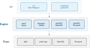
The three tiers. The UI is Qt6 widgets plus the pybind11 scripting surface;
the engine holds the data model, the .chiplet reader, the OpenGL
renderer and the KLayout-backed 2D view. Everything in the bottom row is an
external dependency, and the KLayout entry there is both why a build needs a
KLayout tree and why the licence is GPL-3.0-or-later.
Docker. ./scripts/build-docker.sh builds inside the image and
./scripts/run-docker.sh runs it with display forwarding. Note that a
Docker-built build/chiplet-studio will generally not run directly on the
host; launch it through the scripts.
Manual build. Requires Qt6, yaml-cpp, OpenGL and KLayout libraries. KLayout is a submodule and is built first:
cd extern/klayout && ./build.sh -j$(nproc)
mkdir build && cd build
cmake .. -DKLAYOUT_BUILD_DIR=../extern/klayout/bin-release
make -j$(nproc)
Portable bundle. scripts/build-portable.sh produces a self-contained
tree in dist/ for machines with neither Docker nor root:
./scripts/build-portable.sh             # tarball, bundled software-GL fallback
./scripts/build-portable.sh --appimage  # also emit an AppImage
./scripts/build-portable.sh --lean      # smaller, host OpenGL only
The bundle runs on any glibc 2.35 or newer Linux. It uses the host GPU when it
provides OpenGL 3.3 and otherwise falls back to a bundled llvmpipe software
renderer. Force either with CHIPLET_GL:
CHIPLET_GL=hardware ./AppRun
CHIPLET_GL=software ./AppRun
Resolving PDK roots
Paths inside a .chiplet file may be written with ${VAR} placeholders, and
Chiplet Studio resolves them with the same three-tier discovery the Python side
of the toolchain uses: an environment variable that is set and valid, then a
walk up the parent directories for a sibling checkout, then a loud failure.
Variable |
Sibling directory names |
Marker subpath |
|---|---|---|
|
|
|
|
|
|
|
|
|
|
|
|
|
|
|
The marker subpath is what makes “set and valid” checkable: a variable pointing at a directory that does not contain its marker is treated as unset and the walk continues. This matters in practice, because a stale exported variable is a more common failure than an unset one.
Note
The Docker images bake these variables at fixed container paths, and the
launcher scripts mount host checkouts onto them. Those values exist only
inside the image. Running the tools directly on the host means exporting
INTERPOSER_PDK_ROOT, INTERCONNECT_PDK_ROOT and PDK_ROOT yourself.
The visible symptom of a missing interconnect PDK is that Cu-pillar and bump
bodies do not appear in the interposer’s detailed view.
Known limits
3D pad-name text is not rendered. Pad names appear in the 2D drill-down only.
The
Layer Zexaggeration is restricted to a single imported die.The net graph reads the netlist in the assembly file and performs no extraction, so it shows declared connectivity, not verified connectivity.
Assembly-mode 2D falls back to the interposer’s own layout when no merged assembly GDS exists, which is a labelled fallback rather than a complete view.